 |
|||
|
|
|||
| ||||||||||
|
|  MIL-M-38510/117C
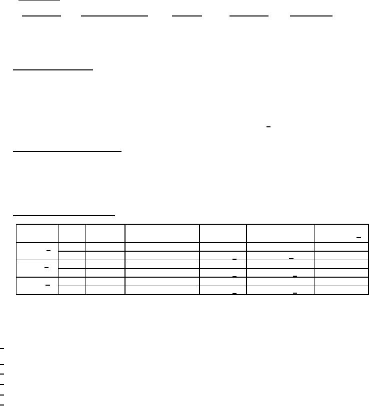
1.2.3 Case outlines. The case outlines are as designated in MIL-STD-1835 and as follows:
Descriptive designator
Terminals
Device types
Package style
Outline letter
X
See figure 1
4
01
Can
Y
See figure 2
4
02
Flange mount
X
See figure 3
3
03
Can
Y
See figure 4
2
04,05,06
Flange mount
1.3 Absolute maximum ratings.
Input voltage (device types 01 and 02) ...........................................................
40 V
Input-output differential voltage
(device types 03 and 04)..............................................................................
40 V
(device types 05 and 06)..............................................................................
35 V
+300C
Lead temperature (soldering, 60 seconds) .....................................................
+150C 1/
Junction temperature (TJ) ...............................................................................
-65C to +150C
Storage temperature range ............................................................................
1.4 Recommended operating conditions.
Input voltage range:
Device types 01 and 02 ..............................................................................
8 V dc to 38 V dc
Device types 03 and 04 ..............................................................................
4.25 V dc to 41.25 V dc
Device types 05 and 06 ..............................................................................
4.25 V dc to 36.25 V dc
-55C to +125C
Ambient operating temperature range (TA) ....................................................
1.5 Power and thermal characteristics.
Maximum PD without
Maximum PD with
Max θJA
Max θJC
Max θC-S 2/
Case
TA = TS
heat sink
heat sink
125C 3/
140C/W
40C/W
10C/W
X
0.18 W
0.5 W
35C/W
4C/W 4/
0.5C/W
Y
0.71 W
5.6 W 5/
25C 3/
140C/W
40C/W
10C/W
X
0.89 W
2.50 W
35C/W
4C/W 4/
0.5C/W
Y
3.60 W
28.00 W 6/
-55C 3/
140C/W
40C/W
10C/W
X
1.50 W
4.00 W
35C/W
4C/W 4/
0.5C/W
Y
5.80 W
45.00 W 6/
______
1/ The device is protected by a thermal shutdown circuit which is designed to turn off the output transistor whenever
the device junction temperature is in excess of 150C.
2/ This value represents the maximum allowable thermal impedance of a heat sink to remain within the thermal ratings.
3/ Based on TJ = 150C and specified values of θJA and θJC.
Maximum θJC at all temperatures (for case Y only) = 1.5C/W for device type 05 and 1.0C/W for device type 06.
4/
Power dissipation (PD) at 125C (for case Y only) = 12.5 W for device type 05 and 16.6 W for device type 06.
5/
Power dissipation (PD) at -55C and +25C (for case Y only) = 30 W for device type 05 and 50 W for device type 06.
6/
2
|
|
Privacy Statement - Press Release - Copyright Information. - Contact Us |
