 |
|||
|
Page Title:
Table 1. Electrical performance characteristics. |
|
||
| ||||||||||
|
| 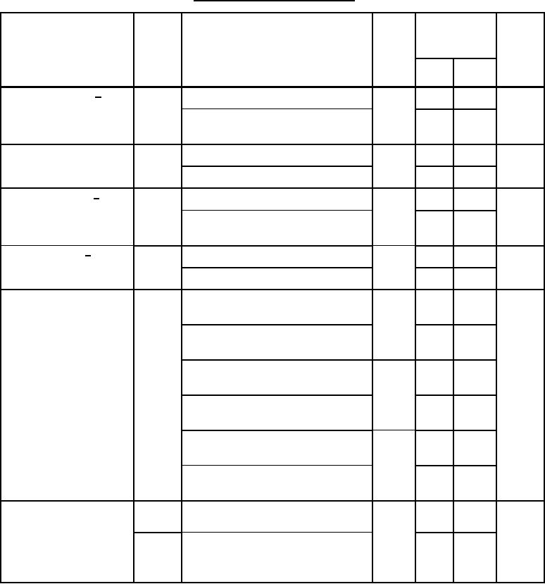 MIL-M-38510/125B
TABLE I. Electrical performance characteristics.
Conditions
Device
Limits
Unit
Test
Symbol
-55C ≤ TA ≤ +125C
type
VCC = 15 V,
see figure 3 and 3.5
Min
Max
unless otherwise specified
01,02
-3
3
mV
Input offset voltage 1/
VIO
VCC = 5 V to 15 V, TA = +25C
-5
5
VCC = 5 V to 15 V,
-55C ≤ TA ≤ +125C
01,02
-20
20
Input offset voltage
V/C
TA = -55C to +25C
ĆVIO /
temperature sensitivity
-20
20
ĆT
TA = +25C to +125C
01,02
-1
25
nA
Input bias current
1/
IIB
VCC = 5 V to 15 V, TA = +25C
-25
75
VCC = 5 V to 15 V,
-55C ≤ TA ≤ +125C
01,02
2
Input impedance 2/
GΩ
ZI
TA = +25C
1
-55C ≤ TA ≤ +125C
Gain error
01,02
-.005
+.005
%
VIN = -11.5 V to +11.5 V, RL = 10 kΩ,
AE
TA = +25C
-0.02
+0.02
VIN = -11.5 V to +11.5 V, RL = 10 kΩ,
-55C ≤ TA ≤ +125C
02
-.005
+.005
VIN = -10 V to +10 V, RL = 2 kΩ,
TA = +25C
-0.02
+0.02
VIN = -10 V to +10 V, RL = 2 kΩ,
-55C ≤ TA ≤ +125C
01,02
-0.02
+0.02
VCC = 5 V, RL = 10 kΩ,
VIN = -2 V to +2 V, TA = +25C
-0.04
+0.04
VCC = 5 V, VIN = -2 V to +2 V,
RL = 10 kΩ, -55C ≤ TA ≤ +125C
Input offset voltage
01,02
+6
mV
VIO
VIN = 0 V, VOFFSET ADJ at +VCC
adjustment
(ADJ+)
-6
VIO
VIN = 0 V,
(ADJ-)
VOFFSET ADJ at 1 kΩ from +VCC,
20 kΩ from 0 V
See footnotes at end of table.
4
|
|
Privacy Statement - Press Release - Copyright Information. - Contact Us |
