 |
|||
|
Page Title:
Table 1. Electrical performance characteristics-cont. |
|
||
| ||||||||||
|
| 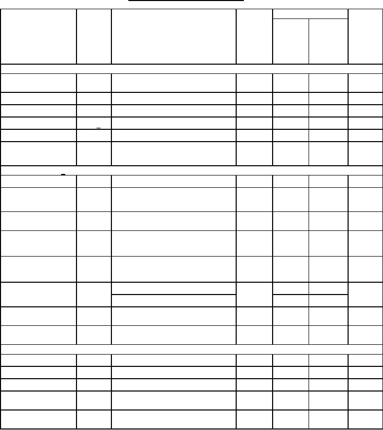 MIL-M-38510/126C
TABLE I. Electrical performance characteristics Continued.
Conditions
Device
Limits
Test
Symbol
type
Units
VIN = 15 V dc, RT = 4.12 kΩ 0.01 %
Min
Max
RD = 0 kΩ, CT = 0.01 F 0.1 %
-55C ≤ TC ≤ +125C
unless otherwise specified
Reference section
Reference output
03
4.9
5.1
V
VREF
voltage
Line regulation
03
-20
20
mV
VRLINE
VIN = 8 V to 35 V
Load regulation
03
-30
30
mV
VRLOAD
ILOAD = 0 to 20 mA
Short circuit current
03
-125
mA
VREF = 0 V, t < 25 ms
IOS 1/
V rms
Output noise voltage
03
200
10 Hz ≤ f ≤ 10 kHz, TC = +25C
NO
Ripple rejection
03
50
dB
ĆVIN /
VIN = 15 V, +1 V rms, TC = +25C,
sinewave at 2.4 kHz
ĆVREF
Oscillator section 6/
Initial frequency
03
38
42
kHz
TC = +25C
fOSC
Voltage stability
03
-1
1
%
ĆfOSC /
8 V ≤ VIN ≤ 35 V
ĆVIN
Oscillator frequency
03
36
44
kHz
TC = -55C, +125C
fOSC2
Minimum frequency
03
100
Hz
RT = 150 kΩ 0.1 %,
fOSC
(MIN)
CT = 0.20 F 1.0 %, RD = 0 kΩ
Maximum frequency
03
350
kHz
RT = 2 kΩ 0.1 %,
fOSC
(MAX)
CT = 1.0 nF 1.0 %, RD = 0 kΩ
s
Clock width
03
2
TC = -55C, +25C
tPW
3
TC = +125C
Sawtooth peak
03
2.5
3.5
V
VRP
VIN = 35 V
voltage
Sawtooth valley
03
0.45
V
VIN = 8 V
VRV
voltage
Error amplifier section
Input offset voltage
03
-5
5
mV
VIO
VCM = 2.5 V
A
Input bias current
03
-1
IIB
VCM = 2.5 V
A
Input offset current
03
-0.5
0.5
IIO
VCM = 2.5 V
Open loop voltage
03
60
dB
AVS
gain
Common mode
CMR
03
70
dB
VCM = 0 to 5.2 V
rejection
See footnotes at end of table.
10
|
|
Privacy Statement - Press Release - Copyright Information. - Contact Us |
