 |
|||
|
Page Title:
Table 3. Group A inspection for device type 01-cont. |
|
||
| ||||||||||
|
| 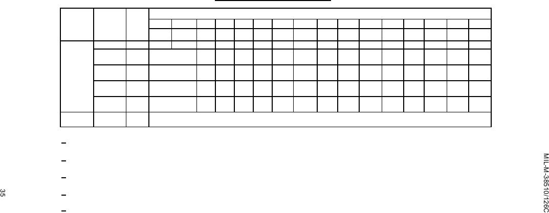 TABLE III. Group A inspection for device type 01 Continued.
Adapter pin numbers
Test no.
1
2
3
4
5
6
7
8
9
10
11
12
13
14
15
16
Subgroup
Symbol
SHUT
GND
COMP
NONINV
OSC
INV
-CL
RT
CT
EA
CA
CB
EB
VIN
VREF
+CL
DOWN
INPUT
INPUT
2 kΩ
.01 F
10
GND
GND
20 V
20 V
GND
20 V
85
2.5 V
2.5 V
GND
GND
tPW
Tc =
86
= 2.5 V
"
"
"
"
"
3.8 V
"
"
"
"
"
tON(A)MAX /
VCM
+125C
tOSC
87
"
"
"
"
"
"
0.5 V
"
"
"
"
"
tON(A)MIN /
tOSC
88
"
"
"
"
"
"
3.8 V
"
"
"
"
"
tON(B)MAX /
tOSC
89
"
"
"
"
"
"
0.5 V
"
"
"
"
"
tON(B)MIN /
tOSC
All test parameters, test conditions, equations, and test limits are identical with those specified in table III, subgroup 10, TC = +125C.
11
90 to
Tc = -55C
94
VOSC = 5 V, 50 s pulse. Pulse VOSC to switch output transistor (which is on).
1/
2/
Measure VCOMP with VN = 1.8 V and VN = 3.4 V.
The capacitor shall be polystyrene 0.01 F tuned with a mica capacitor to 0.1 %.
3/
4/
Adjust V +C.L. sense until VCOMP = 2 V.
5/
See figure 4.
|
|
Privacy Statement - Press Release - Copyright Information. - Contact Us |
