 |
|||
|
Page Title:
Table 3. Group A inspection for device type 06-cont. |
|
||
| ||||||||||
|
| 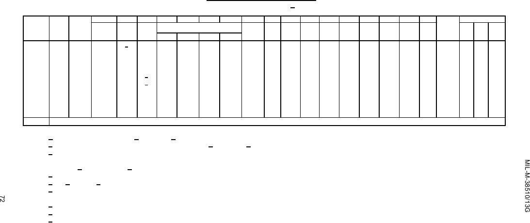 TABLE III. Group A inspection for device type 06 Continued.
Terminal conditions 2/
Case E, F
1
2
3
4
5
6
7
8
9
10
11
12
13
14
15
16
Test limits
MIL-
DATA INPUTS
Subgroup
Symbol
Enable
Enable
Output
Output
Output
Output
Carry
Meas.
STD-883
method
Test No.
Clear
Clock
A
B
C
D
P
GND
Load
T
output
terminal
Min
Max
Unit
VCC
QD
QC
QB
QA
10
tPLH4
Fig 7
195
8/
IN
IN
4.5 V
4.5 V
4.5 V
4.5 V
GND
GND
4.5 V
OUT
5.0 V
3
36
ns
QA
tPLH4
and 7A
196
"
"
4.5 V
IN
4.5 V
4.5 V
"
"
"
"
OUT
"
"
"
"
TC =125C
QB
tPLH4
"
197
"
"
"
4.5 V
IN
4.5 V
"
"
"
"
OUT
"
"
"
"
QC
tPLH4
"
198
"
"
"
"
4.5 V
IN
"
"
"
"
OUT
"
"
"
"
QD
tPLH5
"
199
4.5 V
7/
"
"
"
4.5 V
"
"
"
IN
OUT
"
Carry
"
27
"
tPHL5
"
200
4.5 V
7/
"
"
"
"
"
"
"
IN
OUT
"
Carry
"
27
"
tPHL6
"
201
IN
IN
"
"
"
"
"
"
"
4.5 V
OUT
"
"
47
"
QA
tPHL6
"
202
"
"
"
"
"
"
"
"
"
"
OUT
"
"
"
"
QB
tPHL6
"
203
"
"
"
"
"
"
"
"
"
"
OUT
"
"
"
"
QC
tPHL6
"
204
"
"
"
"
"
"
"
"
"
"
OUT
"
"
"
"
QD
Same tests, terminal conditions and limits as subgroup 10, except TC = -55C.
11
1/ Normal clock pulse: (VIL < 0.8 V, VIH > 2.0 V).
2/ Terminal conditions (pins not designated may be H > 2.0 V, or L < 0.8 V, or open).
3/ Output voltages shall be either:
(a) H = 2.4 volts minimum and L = 0.4 volt maximum when using a high speed checker double comparator, or
(b) H > 1.5 volts and L < 1.5 volts when using a high speed checker single comparator.
4/ Only a summary of attributes data is required.
5/ A > 2.0 V, B < 0.8 V. Input voltages shown are the maximum for VIL and the minimum for VIH.
6/ FMAX, minimum limit specified is the frequency of the input pulse. The output frequency shall be as follows: FMAX/2 at QA, FMAX/4 at QB,
FMAX/8 at QC, FMAX/16 at QD.
7/ Apply 1 clock pulse prior to input pulses.
8/ Apply momentarily GND, then 4.5 volts prior to input pulses, maintain 4.5 volts during test.
9/ Minimum limit for circuit C shall be -0.5 mA.
|
|
Privacy Statement - Press Release - Copyright Information. - Contact Us |
