 |
|||
|
Page Title:
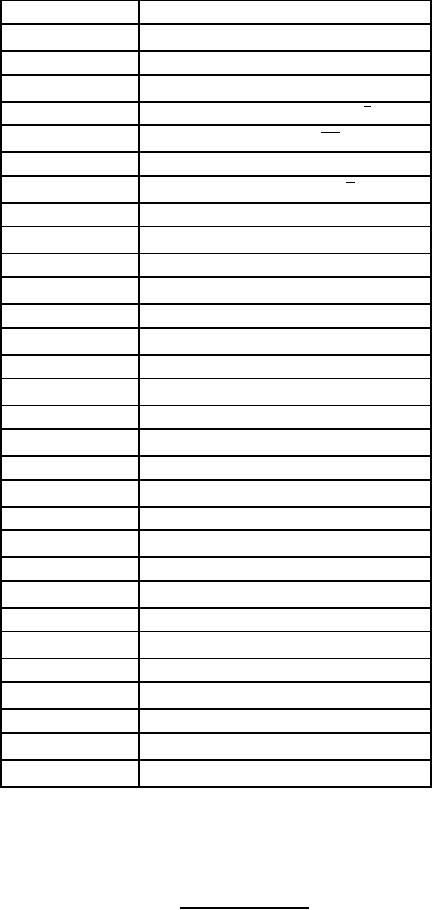
Figure 1. Terminal connections. |
|
||
| ||||||||||
|
|  MIL-M-38510/140A
Device types
01, 02, 03, 04, 05, 06
Case outlines
X, Y, Z
Terminal number
Terminal symbol
1
+5 V SUPPLY (+V LOGIC)
2
DATA MODE SELECT 12 / 8
3
CHIP SELECT CS
4
BYTE ADDRESS A0
5
READ/CONVERT R / C
6
CHIP SELECT CE
7
+12 V / +15 V SUPPLY (+VCC)
8
+10 V REF OUT
9
ANALOG GND (SEE NOTE)
10
+10 V REF IN
11
-12 V / -15 V SUPPLY (VEE)
12
BIPOLAR OFFSET
13
10 V INPUT
14
20 V INPUT
15
DIGITAL GND (SEE NOTE)
16
DB 0 (LSB)
17
DB 1 (BIT 11)
18
DB 2 (BIT 10)
19
DB 3 (BIT 9)
20
DB 4 (BIT 8)
21
DB 5 (BIT 7)
22
DB 6 (BIT 6)
23
DB 7 (BIT 5)
24
DB 8 (BIT 4)
25
DB 9 (BIT 3)
26
DB 10 (BIT 2)
27
DB 11 (MSB)
28
STATUS OUTPUT
NOTE: The units two ground pins (pins 9 and 15) must be connected together as close to the package
as possible, and preferably should be connected to a large analog ground plane underneath
the package. If these commons must be run separately, a non-polarized 0.01 F bypass capacitor
should be connected between pins 9 and 15 as close to the unit as possible and wide conductor runs
should be employed.
Figure 1. Terminal connections.
14
|
|
Privacy Statement - Press Release - Copyright Information. - Contact Us |