 |
|||
|
Page Title:
Figure 4. Switching test circuit and data to output waveforms for device types 01 and 02. |
|
||
| ||||||||||
|
| 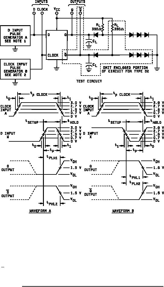 MIL-M-38510/15B
NOTES:
1. The D input pulse generator has the following characteristics: VGEN = 3 V, t1 = t0 ≤ 10 ns, tP = 30 ns, t(SETUP) =
25 ns, t(HOLD) = 5 ns, PRR = 1 MHz and ZOUT ≈ 50 Ω.
2. The clock pulse generator has the following characteristics: VGEN = 3 V minimum, t1 = t0 ≤ 10 ns, tP(CLOCK) =
500 ns, and PRR = 1 MHz.
3. Prior to testing the device shall be precondition to a high logic level for waveform A and to a low logic level for
waveform B.
4. Each latch is tested separately.
5. CL = 50 pF, which includes probe and jig capacitance.
6. RL = 390 Ω 5%.
7.
The Q waveforms are not applicable to type 02.
8.
All diodes are 1N3064 or equivalent.
Figure 4. Switching test circuit and data to output waveforms for device types 01 and 02.
13
|
|
Privacy Statement - Press Release - Copyright Information. - Contact Us |
