 |
|||
|
Page Title:
Figure 5. Synchronous switching test circuit (low level data) for device types 01 and 02. |
|
||
| ||||||||||
|
| 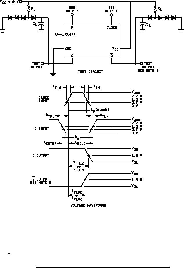 MIL-M-38510/17B
NOTES:
1. Clock input has the following characteristics: Vgen = 3 V minimum, tP = 20 ns, tTHL = tTLH ≤ 10 ns, and
PRR ≤ 1 MHz. When testing fMAX PRR = 25 MHz.
2. D input pulse has the following characteristics: Vgen = 3 V minimum, tTHL = tTLH ≤ 10 ns, tP = 30 ns,
tSETUP = 25 ns, tHOLD = 5 ns and PRR ≤ 0.5 MHz. When testing fMAX PRR = 12.5 MHz at 50% 15% duty
cycle.
3. RL = 390 Ω 5%; CL = 50 pF 10% (including jig and probe capacitance).
4. All diodes are 1N3064 or equivalent.
5.
Q output applies to device type 02 only.
Figure 5. Synchronous switching test circuit (low level data) for device types 01 and 02.
12
|
|
Privacy Statement - Press Release - Copyright Information. - Contact Us |
