 |
|||
|
Page Title:
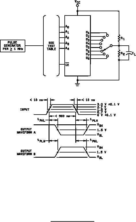
Figure 4. Switching time test circuit. |
|
||
| ||||||||||
|
|  MIL-M-38510/207E
NOTES:
1. Test table for devices programmed in accordance with an altered item drawing may be replaced by the
equivalent tests which apply to the specific program configuration for the resulting read-only memory.
2. CL = 30 pF minimum, including jig and probe capacitance; R1 = 330 Ω 25% and R2 = 680 Ω 20 %.
3. Outputs may be under load simultaneously.
FIGURE 4. Switching time test circuit.
10
|
|
Privacy Statement - Press Release - Copyright Information. - Contact Us |
