 |
|||
|
Page Title:
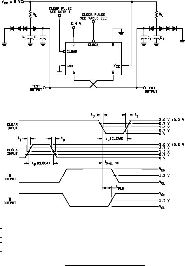
Figure 6. Clear switching test circuit for device types 03. |
|
||
| ||||||||||
|
|  MIL-M-38510/21F
NOTES:
1/ Clear input pulse characteristics: Vgen = 3.0 V 0.2 V, t0 = 15 ns, t1 = 15 ns, tP(CLEAR) = 100 ns,
PRR = 0.5 MHz and ZOUT = 50 Ω.
2/ CL = 50 pF minimum and includes probe and jig capacitance.
3/ RL = 4 kΩ 5% and C1 = 30 pF minimum.
4/ All diodes are 1N916 or equivalent.
5/ Clock input pulse characteristics: Vgen = 3.0 V 0.2 V, tP(CLOCK) ≥ 200 ns, PRR = 0.5 MHz.
FIGURE 6. Clear switching test circuit for device types 03.
18
|
|
Privacy Statement - Press Release - Copyright Information. - Contact Us |
