 |
|||
|
Page Title:
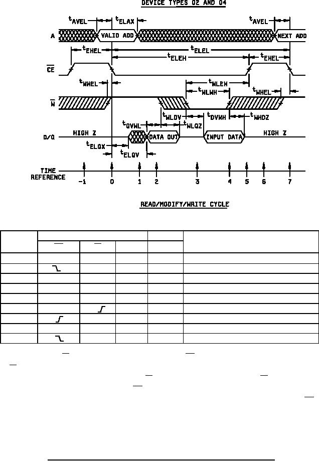
Figure 4. Read cycle, write cycle, read/modify/write cycle waveforms and truth tables Device types 02 and 04-cont. |
|
||
| ||||||||||
|
|  MIL-M-38510/245B
TRUTH TABLE
Inputs
Data I/O
Function
Time
reference
A
DQ
W
CE
H
X
-1
X
Z
Memory disable
0
H
V
Z
Cycle begins, addresses are latched
1
L
H
X
X
Read mode, output enabled
2
L
H
X
V
Read mode, output valid
3
L
L
X
Z
Write mode, output high Z
4
L
X
V
Write mode, data is written
5
H
X
Z
Write completed
6
H
X
X
Z
Prepare for next cycle (same as -1)
7
H
V
Z
Cycle ends, next cycle begins (same as 0)
If the pulse width of W is relatively short in relation to that of CE , a combination read-write cycle may be performed.
If W remains high for the first part of the cycle, the outputs will become active during time (T = 1). Data out will be
valid during time (T = 2). After the data is read, W can go low. After minimum tWLWH, W may return high. The
information just written may now be read or CE may return high, disabling the output buffers and preparing the
device for the next cycle. Any number or sequence of read-write operations may be performed while CE is low
providing all timing requirements are met .
NOTE: See figure 5 for test conditions.
FIGURE 4. Read cycle, write cycle, read /modify/write cycle waveforms and truth tables Continued.
22
|
|
Privacy Statement - Press Release - Copyright Information. - Contact Us |
