 |
|||
|
Page Title:
Figure 11. Synchronous switching test circuit (high level data) for device types 05 and 07. |
|
||
| ||||||||||
|
| 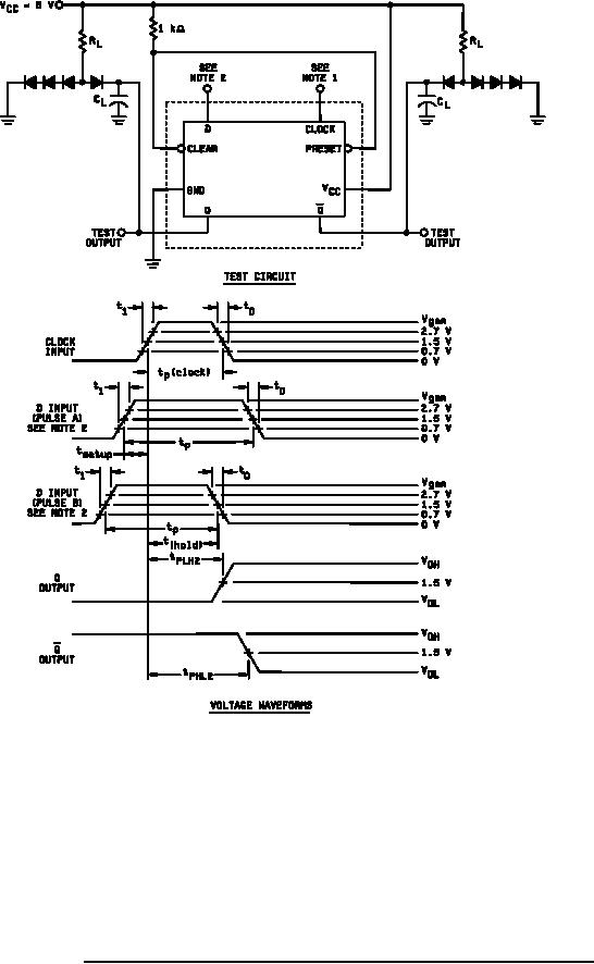 MIL-M-38510/2G
NOTES:
1. Clock input pulse has the following characteristics: Vgen = 3 V, to = t1 ≤ 10 ns, tp (clock) = 30
ns, and PRR = 1 MHz. When testing fMAX, PRR = see table III.
2. D input (pulse A ) has the following characteristics: Vgen = 3 V, to = t1 ≤ 10 ns, tSETUP = 25 ns,
tp = 60 ns, and PRR is 50% of the clock PRR. D input (pulse B) has the following
characteristics: Vgen = 3 V, to = t1 < 7 ns, thold = 6 ns, tp = 60 ns, and PRR is 50% of the clock
PRR.
3. All diodes are 1N3064, or equivalent.
4. CL = 50 pF minimum (including jig and probe capacitance).
5. RL = 390Ω 5%
FIGURE 11. Synchronous switching test circuit (high level data) for device types 05 and 07.
30
|
|
Privacy Statement - Press Release - Copyright Information. - Contact Us |
