 |
|||
|
Page Title:
Table 3. Group A inspection for device type 07-cont. |
|
||
| ||||||||||
|
| 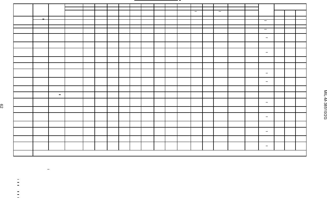 TABLE III. Group A inspection for device type 07. 1/ - Continued.
Subgroup
Symbol
MIL-STD-
Test limits
Case A, B D
1
2
3
4
5
6
7
8
9
10
11
12
13
14
883
Meas.
Case C
3
2
1
14
13
12
11
10
9
8
7
6
5
4
method
terminal
Test No.
Clock
D1
Clear
VCC
Clear
D2
Clock
Preset
Q2
GND
Q1
Preset
Min
Max
Unit
Q2
Q1
1
1
2
2
2
1
10
FMAX 6/
(Fig. 11)
102
IN
E
5.0 V
5.0 V
GND
OUT
5.0 V
Q1
10
MHz
TC = 125C
"
"
103
IN
E
5.0 V
"
"
OUT
5.0 V
"
"
Q1
"
"
"
104
"
5.0 V
E
IN
5.0 V
OUT
"
Q2
"
"
"
"
"
105
"
5.0 V
E
IN
5.0 V
OUT
"
"
"
Q2
"
tPLH
3003
106
IN
"
"
OUT
IN
Clear 1
5
31
ns
((Fig. 10)
to Q 1
"
"
107
IN
"
"
OUT
IN
Preset 1
"
"
to Q1
"
"
"
108
"
IN
IN
OUT
"
Clear 2
"
"
"
to Q 2
"
"
"
109
"
IN
IN
OUT
"
Preset 2
"
"
"
to Q2
"
tPHL
"
110
IN
"
"
OUT
IN
Clear 1
"
39
"
to Q1
"
"
111
IN
"
"
OUT
IN
Preset 1
"
42
"
to Q 1
"
"
"
112
"
IN
IN
OUT
"
Preset 2
42
"
"
to Q 2
"
"
"
113
"
IN
IN
OUT
"
Clear 2
"
39
"
to Q2
"
tPLH
3003 5/
114
IN
IN (A)
B
"
"
OUT
5.0 V
Clock 1
5
31
ns
(Fig. 11)
to Q1
"
"
(Fig. 12)
115
IN
IN (A)
5.0 V
"
"
OUT
B
Clock 1
"
"
"
to Q 1
"
"
(Fig. 11)
116
"
B
IN (A)
IN
5.0 V
OUT
"
Clock 2
"
"
"
to Q2
"
"
(Fig. 12)
117
"
5.0 V
IN (A)
IN
B
OUT
"
Clock 2
"
"
"
to Q 2
"
tPHL
(Fig. 12)
118
IN
IN (B)
5.0 V
"
"
OUT
B
Clock 1
"
39
"
to Q1
"
"
(Fig. 11)
119
IN
IN (B)
B
"
"
OUT
5.0 V
Clock 1
"
"
"
to Q 1
"
"
(Fig. 12)
120
"
5.0 V
IN (B)
IN
B
OUT
"
Clock 2
"
"
"
to Q2
"
"
(Fig. 11)
121
"
B
IN (B)
IN
5.0 V
OUT
"
Clock 2
"
"
"
to Q 2
Same tests, terminal conditions and limits as for subgroup 10, except TC = -55C.
11
NOTES:
A = Normal clock pulse.
B = Momentary GND, then 4.5 V.
E = Input D connected to Q .
1/ Terminal conditions (pins not designated may be H ≥ 2.0 V, or L ≤ 0.8 V, or open).
2/ Input voltages shown are: A = 2.0 V minimum and B = 0.8 V maximum.
3/ Output voltages shall be either: (a) H = 2.4 V, minimum and L = 0.4 V, maximum when using a high speed checker double comparator; or (b)
H ≥ 1.5 V and L < 1.5 V when using a high speed checker single comparator.
4/ Tests shall be performed in sequence.
5/ Tests shall be performed for both D input pulses (A and B).
6/ FMAX, minimum limit specified is the frequency of the input pulse. The output frequency shall be one-half of the input frequency.
|
|
Privacy Statement - Press Release - Copyright Information. - Contact Us |
