 |
|||
|
Page Title:
Table 3. Group A inspection for device type 07-cont. |
|
||
| ||||||||||
|
|  FOOTNOTES:
2.5 V minimum/5.5 V maximum
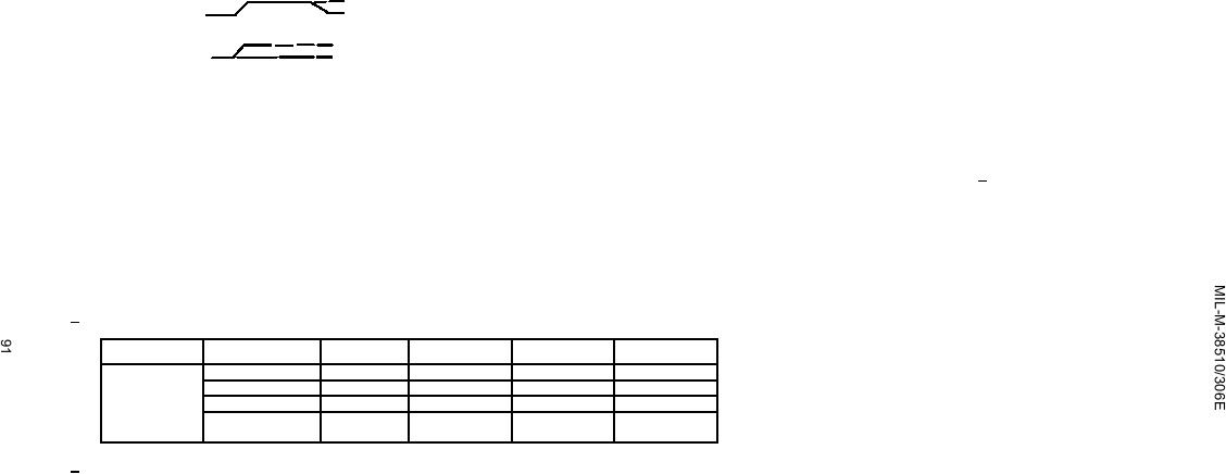
A. Apply input pulse:
0 V-
B. Apply input pulse:
2.5 V minimum/5.5 V maximum.
0V
C. VIN = 2.4V.
D. VIN = 0.4 V.
E. Test numbers 62 through 87 shall be run in sequence.
F. Output voltages shall be either: (1) H ≥2.5 V minimum and L ≤0.4 V maximum when using a high speed checker double comparator: (2) H ≥1.5 V and L <1.5 V when using a high
speed checker single comparator.
G. fMAX minimum limit specified is the frequency of the clock input pulse. The output frequency shall be one-half of the input clock frequency. The input frequency on the parallel input
shall be one-half of the clock input frequency and the parallel input shall be shifted such that the parallel input ↑ and ↓ are coincident with the clock ↑ . Rise and fall times ≤ 6 ns.
Input peak voltage 3 to 5 volts.
J. 3.0 V minimum/5.0 V maximum.
1/ IIL limits (mA) min/max values for circuits shown:
Parameter
Terminal
A
B
C
D
IIL1
Serial
-.075/-.250
-.16/-.40
-.105/-.345
-.12/-.36
AIN, BIN, CIN
-.12/-.36
"
-.105/-.345
-.12/-.36
DIN
-.16/-.40
"
-.16/-.40
-.105/-.345
CLR, Load,
-.16/-.40
-.03/-.30
-.12/-.36
-.12/-.36
CONT, CLK
2/ IOS limits for circuit A for QA through QD are -30 to -130 mA, for QD' is -20 to -100 mA, and for circuits B, C, and D
are -15 to -100 mA.
|
|
Privacy Statement - Press Release - Copyright Information. - Contact Us |
