 |
|||
|
Page Title:
Table 1. Electrical performance characteristics. |
|
||
| ||||||||||
|
| 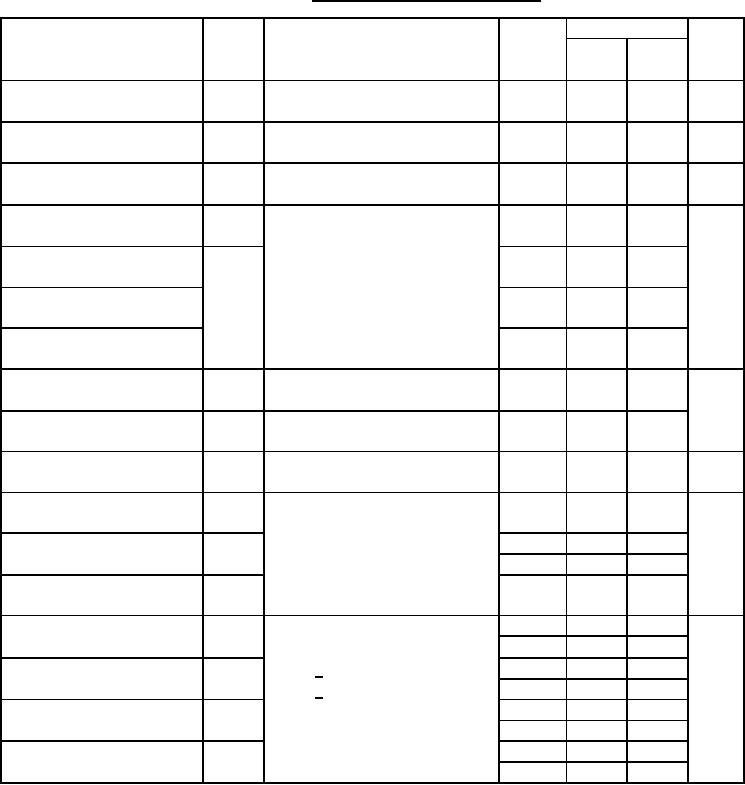 MIL-M-38510/314C
TABLE I. Electrical performance characteristics.
Test
Symbol
Conditions
Device
Limits
Unit
-55C ≤ TC ≤ +125C
types
Min
Max
unless otherwise specified
High level output voltage
VOH
VCC = 4.5 V, VIL = 0.7 V,
All
2.5
V
VIH = 2.0 V, IOH = -400 A
Low level output voltage
VOL
VCC = 4.5 V, VIL = 0.7 V,
All
0.4
V
VIH = 2.0 V, IOL = 4 mA
Input clamp voltage
VIC
VCC = 4.5 V, IIN = -18 mA,
All
-1.5
V
TC = +25C
A
Low level input current
IIL1
VCC = 5.5 V, VIN = 0.4 V
01, 03
-160
-400
Low level input current
IIL2
02
-30
-680
at clear input
Low level input current at AIN
02
-30
-400
Low level input current BIN
02
-30
-580
A
High level input current
IIH1
VCC = 5.5 V, VIN = 2.7 V
All
20
High level input current
IIH2
VCC = 5.5 V, VIN = 5.5 V
All
100
Short circuit output current
IOS
VCC = 5.5 V, VIH = 5.5 V,
All
-15
-130
mA
VIL = GND
Supply current (quiescent)
ICC1
VCC = 5.5 V
02
11
mA
Supply current (quiescent or
ICC2
01
20
triggered)
03
11
Supply current (triggered)
ICC3
02
27
Propagation delay time low to
tPLH1
VCC = 5.0 V
01, 03
5
57
ns
CL = 50 pF 5%, RL = 2 kΩ 5%
02
5
113
high level from input A
Propagation delay time low to
tPLH2
Cext = 1/
01, 03
5
74
high level from input B
Rext = 1/
02
5
90
Propagation delay time low to
tPLH3
01, 03
5
75
high level from clear
02
5
105
Propagation delay time
tPHL1
01, 03
5
75
high to low level from input A
02
5
128
See footnotes at end of table.
5
|
|
Privacy Statement - Press Release - Copyright Information. - Contact Us |
