 |
|||
|
Page Title:
Figure 2. Truth table and functional description. |
|
||
| ||||||||||
|
| 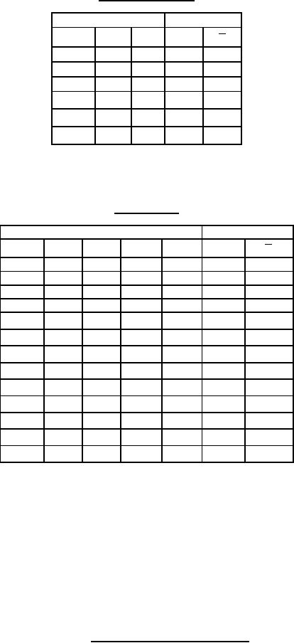 MIL-M-38510/314C
Device type 01 and 02
INPUTS
OUTPUTS
CLEAR
A
B
Q
Q
L
X
X
L
H
X
H
X
L
H
X
X
L
L
H
┌┐
└┘
↑
H
L
┌┐
└┘
↓
H
H
┌┐
└┘
↑
L
H
Device type 03
INPUTS
OUTPUTS
CLEAR
A1
A2
B1
B2
Q
Q
L
X
X
X
X
L
H
X
H
H
X
X
L
H
X
X
X
L
X
L
H
X
X
X
X
L
L
H
┌┐
↑
H
H
L
X
└┘
┌┐
↑
H
L
X
H
└┘
┌┐
↑
H
X
L
H
└┘
┌┐
↑
H
X
L
H
└┘
┌┐
↓
H
H
H
H
└┘
┌┐
↓
↓
H
H
H
└┘
┌┐
↓
H
H
H
H
└┘
┌┐
↑
L
X
H
H
└┘
┌┐
↑
X
L
H
H
└┘
NOTES:
1. H = high level (steady state), L = low level (steady state), ↑ = transition from low to high level,
↓ = transition from high to low level, ┌┐ = one high level pulse, └┘ = one low level pulse,
X = irrelevant (any input, including transitions).
2.
To use the internal timing resistor of device type 03 connect Rint to VCC.
3.
An external timing capacitor may be connected between Cext and Rext/Cext (positive).
4.
For accurate repeatable pulse widths, connect an external resistor between Rext/Cext and
VCC with Rint open circuited.
5.
To obtain variable pulse widths, connect external variable resistance between Rint or Rext/Cext and VCC.
FIGURE 2. Truth table and functional description.
11
|
|
Privacy Statement - Press Release - Copyright Information. - Contact Us |
