 |
|||
|
Page Title:
Table III. Group A inspection for device type 01. (cont) |
|
||
| ||||||||||
|
|  1/
Cases 2 and X pins not referenced are N/C.
2/
Apply all voltages, then apply 4.5 V, 0 V, 4.5 V to SD X, then apply 4.5 V, 0 V, 4.5 V to CPX, then make measurement. Alternate clock:
Apply all voltages, then apply 4.5 V, 0 V, 4.5 V to SD X, then apply 0 V, 4.5 V, 0 V to CPX, then make measurement.
3/
Apply all voltages, then apply 4.5 V, 0 V, 4.5 V to CD X, then apply 4.5 V, 0 V, 4.5 V to CPX, then make measurement. Alternate clock:
Apply all voltages, then apply 4.5 V, 0 V, 4.5 V to CD X, then apply 0 V, 4.5 V, 0 V, to CPX, then make measurement.
4/
Apply all voltages, then apply 0, 4.5 V, 0, to CPX then make measurement.
5/
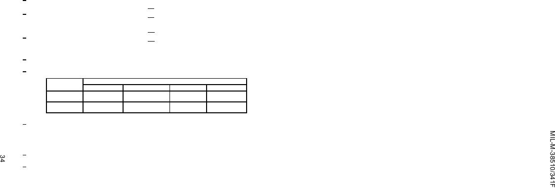
IIL limits (mA) min/max values for circuits shown:
Circuits
Parameter
A
B
C
D
IIL1
-.25/-.60
-.03/-.60
-.03/-.60
-.03/-.60
IIL2
-.75/-1.80
-.09/-1.80
-.09/-1.80
-.09/-1.80
6/
A = 2.5 V
B = 0.5 V
H ≥ 1.5 V
L ≤ 1.5 V
7/
Perform function sequence at VCC = 4.5 V and repeat at VCC = 5.5 V.
8/
fMAX minimum limit specified is the frequency of the input pulse. The output frequency shall be
one-half of the input frequency. fMAX shall be measured only under the conditions of initial qualification
and after process or design changes which may affect this parameter. For all other conditions,
fMAX shall be guaranteed, if not tested, to the limits specified in table III, herein.
|
|
Privacy Statement - Press Release - Copyright Information. - Contact Us |
