 |
|||
|
Page Title:
Figure 4. Synchronous switching test circuit (low-level data) types 01 and 02 |
|
||
| ||||||||||
|
| 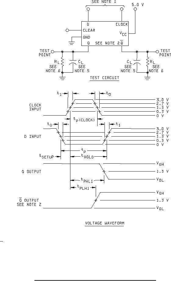 MIL-M-38510/372B
NOTES:
1. Clock input pulse characteristics: t1 = t0 = 6 1.5 ns; PRR ≤ 1.0 MHz.
Q output applies to device type 02 only.
2.
D input pulse characteristics: t1 = t0 = 6 1.5 ns; t(SETUP) = 15 ns; t(HOLD) = 0 ns; PRR is 50% of clock PRR.
3.
4.
Inputs not under test are at ground.
CL = 50 pF 10%, including scope probe, wiring, and stray capacitance without package in test fixture.
5.
RL = 499Ω 1%.
6.
7.
Voltage measurements are to be made with respect to network ground terminal.
FIGURE 4. Synchronous switching test circuit (low-level data) types 01 and 02 - Continued.
15
|
|
Privacy Statement - Press Release - Copyright Information. - Contact Us |
