 |
|||
|
Page Title:
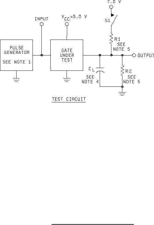
Figure 3. Switching time test circuit for all device types. |
|
||
| ||||||||||
|
|  MIL-M-38510/383B
NOTES:
1. All input pulses are supplied by generators having the following characteristics: t1 = t0 = 6 1.5 ns,
PRR ≤ 1 MHz, ZOUT ≈ 50 Ω.
2. Waveform 1 is for an output with internal conditions such that the output is low except when disabled by the
output control. Waveform 2 is for an output with internal conditions such that the output is high except when
disabled by the output control.
3. In the examples above, the phase relationships between inputs and outputs have been chosen arbitrarily.
4. CL = 50 pF 10%. including scope probe, wiring, and stray capacitance without package in test fixture.
5. R1 = R2 = 499Ω 1%.
6. Voltage measurements are to be made with respect to network ground terminal.
FIGURE 3. Switching time test circuit for all device types.
12
|
|
Privacy Statement - Press Release - Copyright Information. - Contact Us |
