 |
|||
|
Page Title:
Figure 9. FMAX test circuit for device type 03-cont. |
|
||
| ||||||||||
|
| 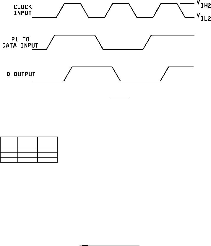 MIL-M-38510/61C
FREQ (IN)
FREQ. (OUT) =
2
FMAX IS HIGHEST INPUT FREQUENCY AT WHICH DEVICE CEASES TO TOGGLE
GENERATOR CHARACTERISTICS
zOUT = 50Ω
VIL2
TC
VIH2
10 mV
10 mV
tTHL = 2.0 ns (20%-80%)
tTLH = 2.0 ns (20%-80%)
25C
+1.11 V +0.31 V
tP (data) = 200 ns
125C
+1.24 V +0.36 V
tP (clock) = 40 ns
-55C
+1.01 V +0.28 V
NOTES:
1. Perform test in accordance with test table; each output is tested separately.
2. All input and output cables are equal lengths of 50 ohm coaxial cables. Wire length should be ≤ .250
(6.35 mm) from tp in to input pin and tp out to output pin.
3. Outputs not under test connected to a 100 ohm resistor to ground.
4. Note that observed pulse amplitude is attenuated by one half.
5. Power supply configuration on MC1660 and MC1662's identical to D.U.T.
FIGURE 9. FMAX test circuit for device type 03 - Continued.
20
|
|
Privacy Statement - Press Release - Copyright Information. - Contact Us |
