 |
|||
|
|
|||
| ||||||||||
|
|  MIL-M-38510/650B
NOTES:
1. Input pins not designated shall be "high" level logic or "low" level logic, or may be left open provided they
do not influence the outcome of the measurement. Output pins not designated shall be tied to the loads
or left open provided they do not influence the outcome of the measurement.
Exceptions are as follows:
a. VIC (POS) tests: The "GND" terminal shall be open. A minimum limit of 0.4 V applies to tests
being performed on equipment not capable of opening "GND" pin during test.
b. VIC (NEG) tests: The VCC terminal shall be open.
c. ICC tests: The output terminals shall be open.
2. See 4.4.1c. All type input terminals (e.g. clock, clear, data, etc.), a minimum of three inputs of each shall
be tested.
3. See 4.4.1d.
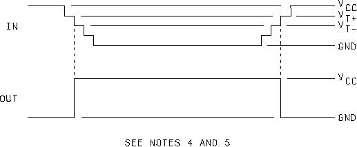
4. Decrement input in 50 mV steps beginning 100 mV above the maximum limit specified until the output
changes from GND to VCC. The input voltage where this transition occurs is VT-.
5. Increment input in 50 mV steps beginning 100 mV below the minimum limit specified until the output
changes from VCC to GND. The input voltage where this transition occurs is VT+.
6. VH = (VT+) (VT-). See table I for VH limits.
32
|
|
Privacy Statement - Press Release - Copyright Information. - Contact Us |
