 |
|||
|
Page Title:
Figure 15. Synchronous switching waveforms and test circuit for device types 05 and 06. |
|
||
| ||||||||||
|
| 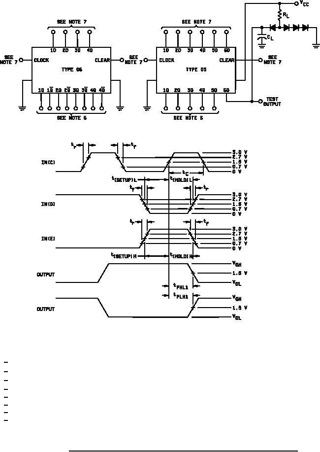 MIL-M-38510/71D
NOTES:
1/ tf = tr ≤ 2.5 ns; IN(C) PRR ≤ 1 MHz, tC = 10 ns.
2/ t(SETUP)L = 7 ns, t(HOLD)L = 5 ns, t(SETUP)H = 7 ns, t(HOLD)H = 5 ns.
3/ CL = 50 pF 10% including jig and probe capacitance.
4/ RL = 280 Ω 5%.
5/ All diodes are 1N3064 or equivalent.
6/ All load circuits are as shown for 6Q.
7/ See table III for input conditions.
8/ Setup and hold time functionally may be verified by separate tests from propagation delay tests by
monitoring the output at specified setup and hold conditions.
FIGURE 15. Synchronous switching waveforms and test circuit for device types 05 and 06.
28
|
|
Privacy Statement - Press Release - Copyright Information. - Contact Us |
