 |
|||
|
Page Title:
Table 1. Electrical performance characteristics-cont. |
|
||
| ||||||||||
|
| 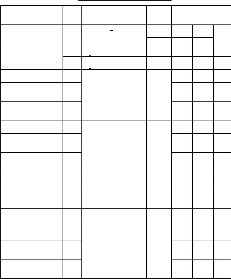 MIL-M-38510/9E
TABLE I. Electrical performance characteristics - Continued.
Device
Limits
Conditions
Test
Symbol
type
-55C ≤ TC ≤ +125C
unless otherwise specified
Supply current
ICC
VCC = 5.5 V
2/
01
72
mA
02
68
04, 05, 06
63
Supply current
ICC1
VCC = 5.5 V, VIN(CLOCK) = 0.4 V
03
44
mA
2/
ICC2
VCC = 5.5 V, VIN(CLOCK) = 2.4 V
03
54
mA
2/
VCC = 5.0 V, CL = 50 pF 10%
Maximum shift frequency
fMAX
01
16
MHz
RL = 400 Ω 5%
Propagation delay time,
tPLH
(See figure 4)
10
42
ns
low to high level from clock 1
or clock 2 to outputs
Propagation delay time,
tPHL
10
49
ns
high to low level from clock 1
or clock 2 to outputs
VCC = 5.0 V, CL = 50 pF 10%
Maximum clock frequency
fMAX
02
7
MHz
RL = 400 Ω 5%
Propagation delay time,
tPLH1
(See figure 5)
8
56
ns
low to high level from clock
to output
Propagation delay time,
tPHL1
8
56
ns
high to low level from clock
to output
Propagation delay time,
tPLH2
8
59
ns
low to high level from preset
to output
Propagation delay time,
tPHL3
8
77
ns
high to low level from clear
to output
VCC = 5.0 V, CL = 50 pF 10%
Maximum clock frequency
fMAX
03
18
MHz
RL = 800 Ω 5%
Propagation delay time,
tPHL1
(See figure 6)
12
63
ns
high to low level, clear input
to Q outputs
Propagation delay time,
tPHL2
10
52
ns
high to low level, clock input
to Q outputs
Propagation delay time,
tPLH2
10
42
ns
low to high level, clock input
to Q outputs
See footnotes at end of table.
7
|
|
Privacy Statement - Press Release - Copyright Information. - Contact Us |
