 |
|||
|
Page Title:
Figure 2. Truth tables and timing diagrams device type 03 |
|
||
| ||||||||||
|
|  MIL-M-38510/9E
Device type 03
SERIAL INPUTS A and B
OUTPUT at tn + 1
INPUTS at tn
A
B
QA
H
H
H
L
H
L
H
L
L
L
L
L
Positive logic:
tn = bit time before clock pulse.
tn + 1 = bit time after clock pulse.
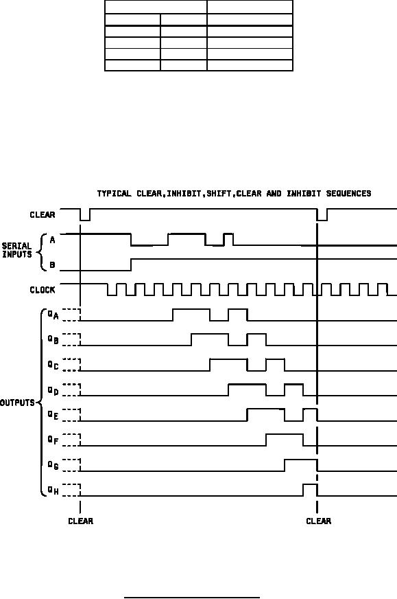
Data at the serial inputs may be changed while the clock is high, but only information meeting the
setup requirements will be entered. Clocking occurs on the low to high level transition of the clock
input.
The clear input is asynchronous. Low level at clear input sets all outputs to logical low.
Figure 2. Truth tables and timing diagrams Continued.
18
|
|
Privacy Statement - Press Release - Copyright Information. - Contact Us |
