 |
|||
|
Page Title:
Table 3. Group A inspection for device type 04-cont. |
|
||
| ||||||||||
|
| 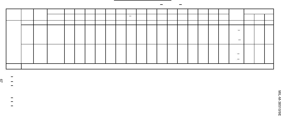 TABLE III. Group A inspection for device type 04 - Continued.
Terminal conditions (pins not designated may be H > 2.0 V or L < 0.8 V or open).
MIL-
Cases E, F
1
2
3
4
5
6
7
8
9
10
11
12
13
14
15
16
Test limits
Meas.
Subgroup
Symbol
STD-883
QH
VCC
QH
SI
A
B
C
D
CLKI
terminal
Min
Max
Unit
method
Test No.
S/L
CLK
E
F
G
H
GND
(Fig 7)
197
IN
IN
GND
GND
GND
GND
GND
OUT
IN
GND
GND
GND
GND
GND
5.0 V
14
MHz
10
QH
fMAX
3003
198
IN
GND
GND
GND
GND
IN
"
OUT
GND
GND
GND
GND
GND
"
10
40
ns
TC = 125C
tPLH1
S/L to QH
(Fig 7)
199
IN
GND
GND
GND
GND
IN
OUT
"
GND
GND
GND
GND
GND
"
"
11
60
"
S/L to QH
tPHL1
"
200
5.0 V
IN
"
OUT
IN
IN
"
"
6
37
"
CLK to QH
tPLH2
"
201
5.0 V
IN
OUT
"
IN
IN
"
"
10
47
"
CLK to QH
tPHL2
"
202
GND
GND
GND
GND
GND
IN
"
OUT
GND
GND
GND
GND
GND
GND
"
5
27
"
"
H to QH
tPLH3
"
203
"
"
"
"
"
"
"
OUT
"
"
"
"
"
"
"
11
54
"
"
H to QH
tPHL3
"
204
"
"
"
"
"
"
OUT
"
"
"
"
"
"
"
"
"
10
41
"
H to QH
tPLH4
"
205
"
"
"
"
"
"
OUT
"
"
"
"
"
"
"
"
10
41
"
"
H to QH
tPHL4
11
Same tests, terminal conditions, and limits as for subgroup 10, except TC = -55 C.
1/ C = after all other input conditions, but prior to measurement, apply momentary GND, then 4.5 V.
2/ For subgroups 7 and 8, A = VCC and B = GND.
3/ Output voltages shall be either:
(a) H = 2.4 V minimum and L = 0.4 V maximum when using a high speed checker double comparator, or
(b) H ≥ 1.5 V and L < 1.5 V when using a high speed checker single comparator.
4/ The tests in subgroups 7 and 8 shall be performed in the sequence specified.
5/ Only a summary of attributes data is required.
6/ For device type 04, schematics incorporating a 4 kΩ base resistor in the clock input circuit, the minimum and maximum limits shall be -0.7 and -1.6 mA, respectively.
For schematics incorporating a 6 kΩ base resistor in the clock input circuit, the minimum and maximum limits shall be -0.4 and -1.3 mA, respectively.
|
|
Privacy Statement - Press Release - Copyright Information. - Contact Us |
