 |
|||
|
Page Title:
Table 3. Group A inspection for device type 06-cont. |
|
||
| ||||||||||
|
| 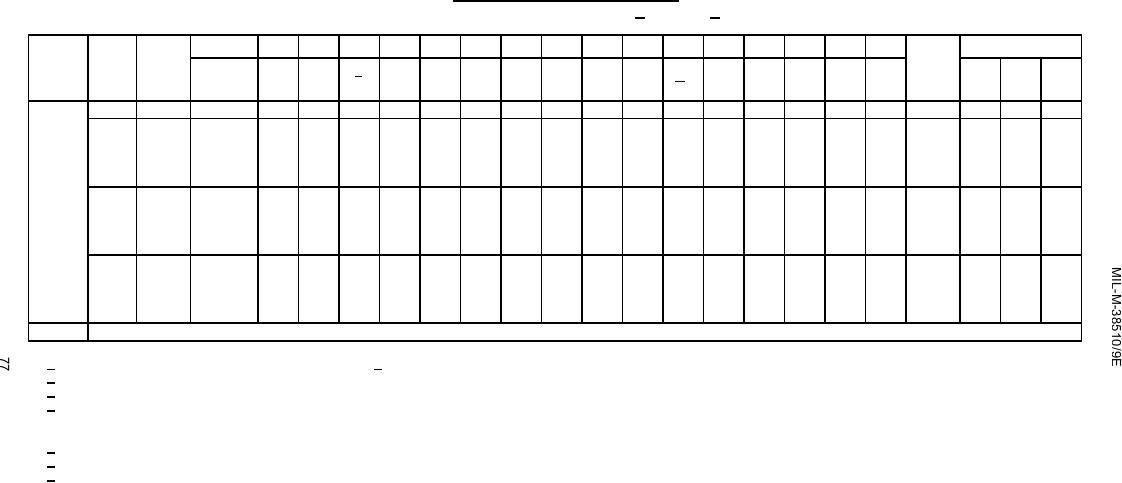 TABLE III. Group A inspection for device type 06 - Continued.
Terminal conditions (pins not designated may be H > 2.0 V or L < 0.8 V or open).
MIL-
Cases E, F
1
2
3
4
5
6
7
8
9
10
11
12
13
14
15
16
Test limits
Subgroup
Symbol
STD-883
Meas.
terminal
Min
Max
Unit
method
Test No.
CLR
J
A
B
C
D
GND
SL
CLK
K
QD
QC
QB
QA
VCC
QD
(Fig 9)
111
B
5.0 V
GND
GND
5.0 V
IN
OUT
5.0 V
12
MHz
10
QA
fMAX
3003
112
IN
5.0 V
5.0 V
5.0 V
5.0 V
GND
GND
"
OUT
"
7
34
ns
TC = 125C
tPHL1
CLR to QA
"
"
(Fig 9)
113
"
"
"
"
"
"
"
"
OUT
"
"
"
"
CLR to QB
"
"
"
114
"
"
"
"
"
"
"
"
OUT
"
"
"
"
CLR to QC
"
"
"
115
"
"
"
"
"
"
"
"
OUT
"
"
"
"
CLR to QD
"
116
B
IN
"
IN
"
OUT
"
"
"
28
"
CLK to QA
tPHL2
"
"
"
117
"
IN
"
"
"
OUT
"
"
"
"
CLK to QB
"
"
"
118
"
IN
"
"
"
OUT
"
"
"
"
CLK to QC
"
"
"
119
"
IN
"
"
"
OUT
"
"
"
"
CLK to QD
"
"
120
"
IN
"
"
"
OUT
"
"
"
34
CLK to QA
tPHL2
"
"
"
121
"
IN
"
"
"
OUT
"
"
"
"
CLK to QB
"
"
"
"
"
"
122
"
IN
"
"
"
OUT
"
CLK to QC
"
"
"
123
"
IN
"
"
"
OUT
"
"
"
"
CLK to QD
2
Same tests, terminal conditions, and limits as subgroup 10 except TC = -55C.
1/
A = normal clock pulse, except for subgroup 7 and 8 (see 3/).
2/
B = momentary GND, then VIN except for subgroups 7 and 8. For subgroups 1, 2 and 3, VIN = VCC; for subgroups 9, 10 and 11, VIN = 3.0 V minimum (see figure 11).
3/
For subgroups 7 and 8, A = VCC and B = GND.
4/
Output voltages shall be either:
(a) H = 2.4 V minimum and L = 0.4 V maximum when using a high speed checker double comparator, or
(b) H ≥ 1.5 V and L < 1.5 V when using a high speed checker single comparator.
5/ The tests in subgroups 7 and 8 shall be performed in the sequence specified.
6/ Only a summary of attributes data is required.
7/ For device type 06, schematic circuits A and B, the minimum and maximum limits shall be -0.4 and -1.3 mA, respectively. For schematic C, the minimum and maximum
limits shall be -0.7 and -1.6 mA, respectively.
|
|
Privacy Statement - Press Release - Copyright Information. - Contact Us |
