 |
|||
|
Page Title:
GCU common zero and zeroing signals switching logic |
|
||
| ||||||||||
|
| 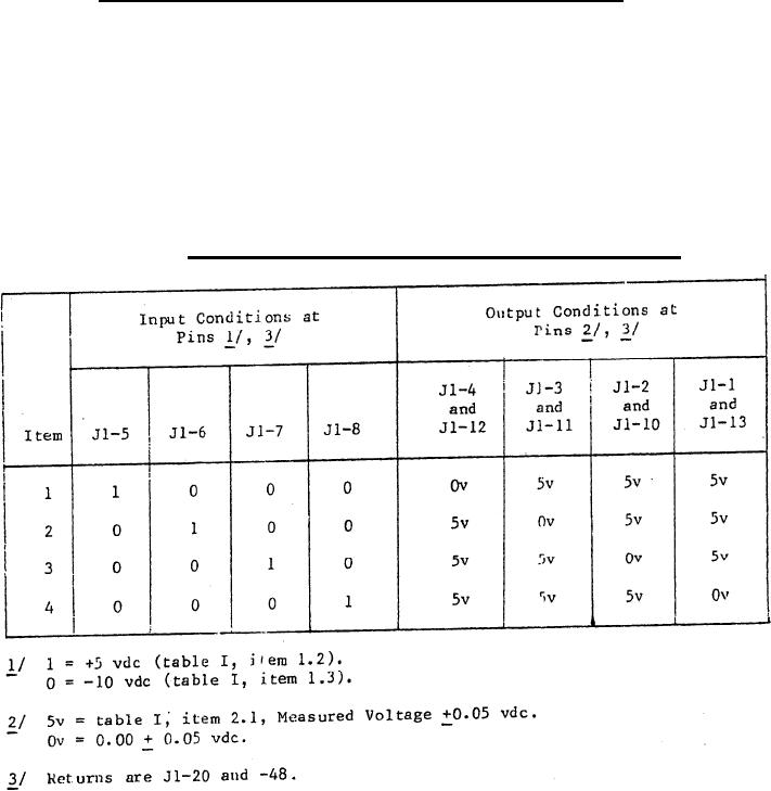 MIL-C-48458B(AR)
3.3.3 GCU common zero and zeroing signals switching logic. With the
interconnections (item 3) and the 5 vdc signal (item 2.1 of table I applied,
and 1.5 vrms signal (item 3.3) of table I applied, establishment, in any item
number order, of the table IV items input conditions shall result in the
corresponding ordered output conditions specified. (See 4.6.2.3)
3.3.4 Fail lamp diodes. With the interconnections (item 3 of table I)
applied and with the 5 vdc signal (item 2.2 of table I) applied in any order
to pins J1-56 through J1-62 and to J1-64, the output at J1-63 shall be 060
0.20 vdc. With the interconnections (item 3 of table I) applied and with the
-5 vdc signal (item 2.3 of table I), applied in any order to pins J1-56 through
J1-62 and to J1-64, the output at J1-63 shall be - 5.00 0.01 vdc. (See
4.6.2.4)
TABLE IV. GCU common zero and zeroing signals switching logic.
7
|
|
Privacy Statement - Press Release - Copyright Information. - Contact Us |
