 |
|||
|
|
|||
| ||||||||||
|
|  MIL-C-50735(MU)
8 August 1973
TABLE III (Continued)
3.3.1.7 B l a n k i n g p u l s e . With the logical zero digital type-A signal
(item 3.1) of table I applied to P1-10, application of the waveform shown
on figure 3 to pin P1-15 shall result in appearance of the output waveforms
shown on figure 3 at the pins specified thereon (the signals may be
recurring)".
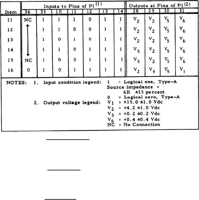
3.3.186 Test switch. With the digital type-A and type-B signals
(items 3.1 and 3.2, respectively) of table I applied as specified in table IV,
the voltages at the output terminals shall be as specified in table IV for
the ass ociated input conditions.
3.3.1.9 C o n t i n u i t y . With neither power nor signals applied, a
short circuit condition (resistance less than 0.3 ohm) shall exist between
P1-33 and Pi-34.
7
|
|
Privacy Statement - Press Release - Copyright Information. - Contact Us |
