 |
|||
|
|
|||
| ||||||||||
|
|  MIL-C-50743(MU)
8 August 1973
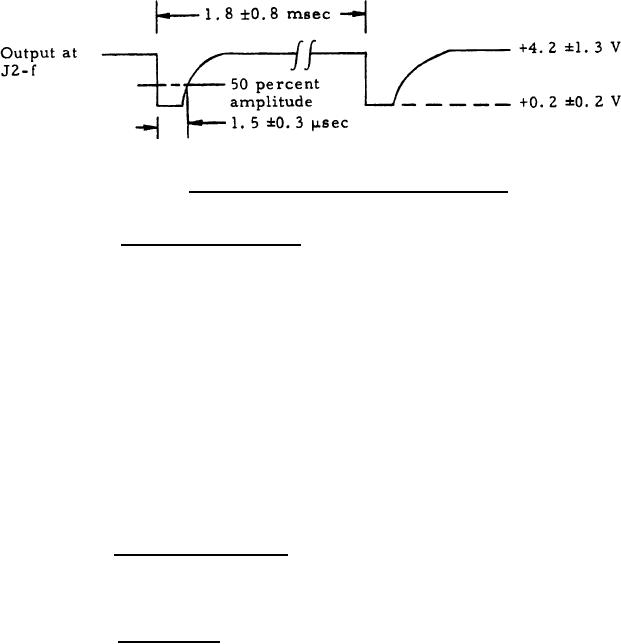
Figure 4. MIN RANGE INHIBIT (2), Waveform
3.3.1.6 A-trigger and video. With the digital type-B signals
(item 3.3 of table I) applied as follows:
a. Logical zero to J1-q, J1-n, and J1-p
b. Logical one to J1-AA, J1-z, J1-m, and J2-h
C.
Momentary logical zero to J1-t, J1-AA, and J1-s
d. Logical zero to J1-z
e. Voltage of J1-r to read +4.2 1.3V
f. Waveforms of figure 5 to the specified pins,
the range readout shall be 9995. When the range readout indicates
9995, the voltage at J1-r shall switch to +0.2 0.2V. If the range
indication is 000 or 9990, the waveforms of figure 5 shall be reapplied.
3.3.1.7 Test access output. With the type-B signal (item 3.3
of table I) applied to the input pins as listed in table IV, the corresponding
outputs shall be as listed in table IV.
3.3.1.8 PFN change. With logical one type-B signals applied
to J1-q, J2-h and J2-d, with a logical zero type-B signal momentarily
applied to J1-t after application of primary power, and with application
of primary power (item 2.1 of table I) the signal waveform of figure 6
shall appear. at J1-w within 4 seconds of application of power and the
waveform at J1-x shall be as shown in figure 6 when the load (item 1.6
of table I) is connected as specified in table I.
10
|
|
Privacy Statement - Press Release - Copyright Information. - Contact Us |
