 |
|||
|
Page Title:
Interface Timing Reference and Delay |
|
||
| ||||||||||
|
|  MIL-D-81347C(AS)
(3) Rise and Fall Time - Except as noted, rise and fall times
are defined as the time for the signal transition between the + 1.75 VDC and +3.50 VDC voltage levels.
All interface signal transitions (rise and fall) shall be less than 150 nanoseconds unless otherwise
specified.
(4) Interface Timing Reference and Delay - The timing refer-
ence for all interface logic signals shall be with respect to the leading edge of the word clock pulse
taken at the connector junction between the MDM and the Drum Controller. The maximum pulse delay
through the Drum Controller as measured at the connector junction points shall be 560 nanoseconds.
(5) Pulse Width and Time Delay Measurements - All pulse
width and time delay measurements on interface signals shall be made where signal transitions cross
the +2. 50 VDC voltage level, unless otherwise specified.
(6) Signal Driver - Except as noted, the signal output driver
circuits used in the MDM shall be capable of providing the specified logic levels, transition times, and
pulse width (or delays) while driving the load (two logic level receivers) as shown in Figure 154.
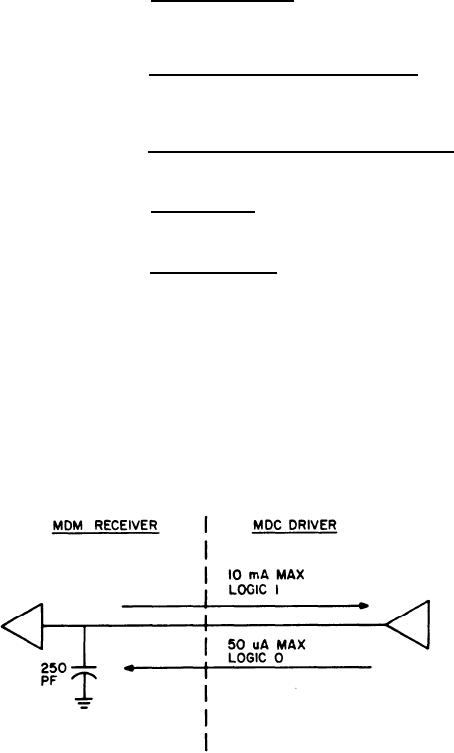
(7) Signal Receivers - The signal receiver inputs to the MDM
shall meet the maximum requirements as stated below and illustrated in Figure 150.
(a) The signal receivers shall require that the driver
sink a maximum of 10 milliamperes to ground for the Logic 1 state.
(b) The signal receivers shall require that the driver
supply a maximum of 50 microampere for the Logic O state.
(c) The signal receiver, including wiring capacitance, shall
present a maximum capacitance of 250 picofarads.
Figure 150. MDM Signal Receiver Requirements
270
|
|
Privacy Statement - Press Release - Copyright Information. - Contact Us |
