 |
|||
|
Page Title:
Table 1. Electrical performance characteristics-cont. |
|
||
| ||||||||||
|
| 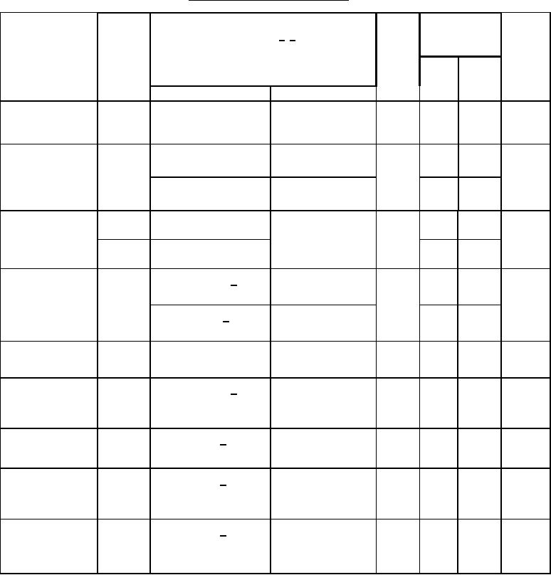 MIL-M-38510/117C
TABLE I. Electrical performance characteristics Continued.
Conditions 1/ 2/
Device
Limits
Unit
Test
Symbol
type
-55C ≤ TA ≤ +125C
see figure 9 and 3.5
Min
Max
unless otherwise specified
Input voltage
Load current
A
03
-5
5
Adjust pin current
-500 mA ≤ IL ≤ -5 mA
ĆIADJ
VIN = 6.25 V
change versus
(LOAD)
load current
Minimum load
03
-3.00
-0.05
mA
4.25 V ≤ VIN ≤ 14.25 V,
IQ
current
forced VOUT = 1.4 V
-5.00
-0.2
VIN = 41.25 V forced
VOUT = 1.4 V
03
-1.8
-0.50
A
Output short
VIN = 4.25 V
IOS1
circuit current
-0.50
-0.05
VIN = 40 V
IOS2
Output voltage
03
1.20
1.30
V
RL = 2.5 Ω,
VIN = 4.25 V,
3/
VOUT
recovery after
(RECOV)
CL = 20 F
after IOS1
1.20
1.30
output short
RL = 250 Ω
VIN = 40 V,
3/
circuit current
after IOS2
Voltage start-up
03
1.20
1.30
V
RL = 2.5 Ω,
VIN = 4.25 V
VSTART
CL = 20 F
Ripple rejection
03
65
dB
ĆVIN /
IL = -125 mA,
VIN = 6.25 V,
4/
ĆVOUT
TA = 25C,
ei = 1 Vrms,
at f = 2400 Hz
see figure 11
Vrms
Output noise
03
120
VNO
VIN = 6.25 V, 4/
IL = -50 mA,
voltage
see figure 12
TA = 25C
Line transient
03
6
mV/V
ĆVOUT /
VIN = 6.25 V, 5/
IL = -10 mA,
response
TA = 25C
ĆVIN
ĆVIN = 3.0 V,
see figure 13
Load transient
03
0.60
mV/mA
ĆVOUT /
VIN = 6.25 V, 5/
IL = -50 mA,
response
see figure 14
ĆIL
ĆIL = -200 mA
TA = 25C
See footnotes at end of table.
10
|
|
Privacy Statement - Press Release - Copyright Information. - Contact Us |
