 |
|||
|
Page Title:
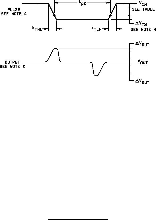
Figure 13. Load transient response test circuit notes |
|
||
| ||||||||||
|
|  MIL-M-38510/118B
NOTES:
1. Heavy current paths (I ≥ 1.0 A) are indicated by bold lines.
2. Kelvin connections must be used for all output current and voltage measurements.
3. The operational amplifier stabilization networks may vary with test adapter construction.
Alternate drive circuits for the 2N6296 may be used to develop the proper load current and input
voltage pulses. These circuits shall require the approval of the qualifying activity.
4. The pulse generator for the pulse load circuit shall have the following characteristics.
(See device table.)
a. Voltage level (VI) = 10 ( |IL| - (VOUT / (R1 + R2)) volts.
Pulse width (tp2) = 25 s.
b.
c.
Duty cycle = 3% (maximum).
tTHL = tTLH = 1.0 s for device types 01 and 02.
d.
tTHL = tTLH = 5.0 s for device types 03 and 04.
e.
Difference voltage level (ĆVI) = 10 (IL) volts.
f.
ĆVOUT = 500 mV maximum for device type 01.
5.
a.
ĆVOUT = 1,000 mV maximum for device type 02.
b.
ĆVOUT = 60 mV maximum for device types 03 and 04.
c.
(These values guarantee the specified limits for load transient response.)
6.
The oscilloscope shall have a bandwidth between 5 and 15 MHz.
FIGURE 13. Load transient response test circuit Continued.
31
|
|
Privacy Statement - Press Release - Copyright Information. - Contact Us |
