 |
|||
|
Page Title:
Table 3. Group A inspection for all device types-cont. |
|
||
| ||||||||||
|
| 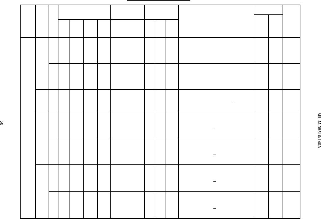 TABLE III. Group A inspection for all device types Continued.
Applied voltages ref. pin 9
DUT digital
Measurement
(figures 4, 5)
output code-word
sense lines
Equation and notes
Limits
Units
ref. pin 9
Subgroup Symbol Test
Min
Max
27 <-------------> 16
7
11
1
13
Pin
Value
Unit
no.
VEE
VDD
VCC
MSB <------------> LSB
VIN(a)
(V)
(V)
(V)
(V)
9
Device types 01,02
100
ns
608
+15.0
-15.0
+5.0
Max (-)
0000 00000 0000
27
t26
ns
Device types 03,04,05,06
150
"
TA =
tHL
tHL1 = t26
25C
Hi-Z delay, referenced to
"
"
609
"
"
"
"
"
"
"
22
t27
"
tHL2 = t27
610
"
"
"
"
"
"
"
16
t28
"
CE high to low transition
"
"
tHL3 = t28
Device types 01,02
100
"
611
"
"
"
Max (+)
1111 1111 1111
27
t29
"
Device types 03,04,05,06
150
"
tHL4 = t29
612
"
"
"
"
"
"
"
22
t30
"
Hi-Z delay, referenced to
"
"
tHL5 = t30
613
"
"
"
"
"
"
"
16
t31
"
CE high to low transition
"
"
tHL6 = t31
614
"
"
"
Max (-)
0000 00000 0000
22
t32
ns
All device types
600
"
tDS
tDS1a
STS low to high transition,
"
"
"
"
referenced to R/ C high
to low transition
615
"
"
"
Max (-)
0000 00000 0000
27
t33
"
All device types
250
"
tDDR
tDDR1 = t33
616
"
"
"
"
"
"
"
22
t34
"
Data valid, referenced to
"
"
tDDR2 = t34
"
"
617
"
"
"
"
"
"
"
16
t35
"
tDDR3 = t35
R/ C low to high transition
618
"
"
"
Max (+)
1111 1111 1111
27
t36
"
All device types
"
"
tDDR4 = t36
619
"
"
"
"
"
"
"
22
t37
"
Data valid, referenced to
"
"
tDDR5 = t37
"
"
620
"
"
"
"
"
"
"
16
t38
"
tDDR6 = t38
R/ C low to high transition
621
"
"
"
Max (-)
0000 00000 0000
27
t39
"
All device types
25
"
tHDR
tHDR1 = t39
622
"
"
"
"
"
"
"
22
t40
"
Data valid, referenced to
"
"
tHDR2 = t40
"
"
623
"
"
"
"
"
"
"
16
t41
"
tHDR3 = t41
R/ C high to low transition
All device types
"
"
624
"
"
"
Max (+)
1111 1111 1111
27
t42
"
tHDR4 = t42
625
"
"
"
"
"
"
"
22
t43
"
Data valid, referenced to
"
"
tHDR5 = t43
"
"
626
"
"
"
"
"
"
"
16
t44
"
tHDR6 = t44
R/ C high to low transition
|
|
Privacy Statement - Press Release - Copyright Information. - Contact Us |
