 |
|||
|
|
|||
| ||||||||||
|
|  MIL-M-38510/140A
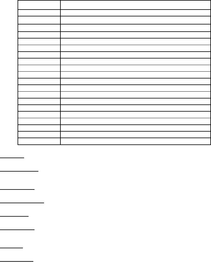
Symbol
Description
R/C
Read and convert, not
Ri
Input resistance of the analog input
STS
Status
Ambient temperature
TA
Conversion time
tc
Data access time from CE high
tdd
Data access time from R/C high
tDDR
Status delay high from R/C low
tDS
Status delay high from CE high
tDSC
Data valid delay from CE low
tHD
Three state output delay from R/C low
tHDR
Three state output delay from CE low
tHL
Status delay low from data valid
tHS
VFSR
Full scale voltage range
Analog input voltage
VIN(a)
Digital output voltage
VO
Digital high level output voltage
VOH
Digital low level output voltage
VOL
Reference output voltage
VREF
12/8
12 or 8 bit parallel output enable control
Bipolar mode. Bipolar mode is the D/A converter operation mode that provides both positive and negative output voltages in
response to an offset binary input code.
Integral linearity error. Integral linearity error is the difference between the average of two input analog voltages, required to
establish adjacent output code-word transitions, with respect to the ideal voltage at the same bit mid point as defined by a
straight line that passes through points extrapolated one half LSB from the first and the last bit transitions.
Differential linearity. Differential linearity is the difference between two input analog voltages required to establish adjacent
output code word transitions. The ideal differential linearity is 1 LSB.
Differential linearity error. Differential linearity error is the difference between the actual and the ideal differential linearity values
for any two adjacent code word transitions.
Full scale range. Full scale range is the voltage difference between the input voltages at the first bit transition and the last bit
transition plus twice the voltage difference between two adjacent bit transitions.
Least significant bit. The least significant bit is the bit in the output code that carries the least weight. The value of the least
significant bit is the average difference between the analog input voltages at two adjacent output bit transitions. The ideal
difference voltage is the value of the full scale range divided by 1024.
Monotonicity. A device is monotonic if the ratio of the incremental change in output to incremental change in input does not
change polarity over the full scale range.
Most significant bit. The most significant bit is the bit in the output code that carries the most weight. It is the output bit that
changes state when the analog input voltage change from its most positive value to one-half of the full scale range.
54
|
|
Privacy Statement - Press Release - Copyright Information. - Contact Us |
