 |
|||
|
Page Title:
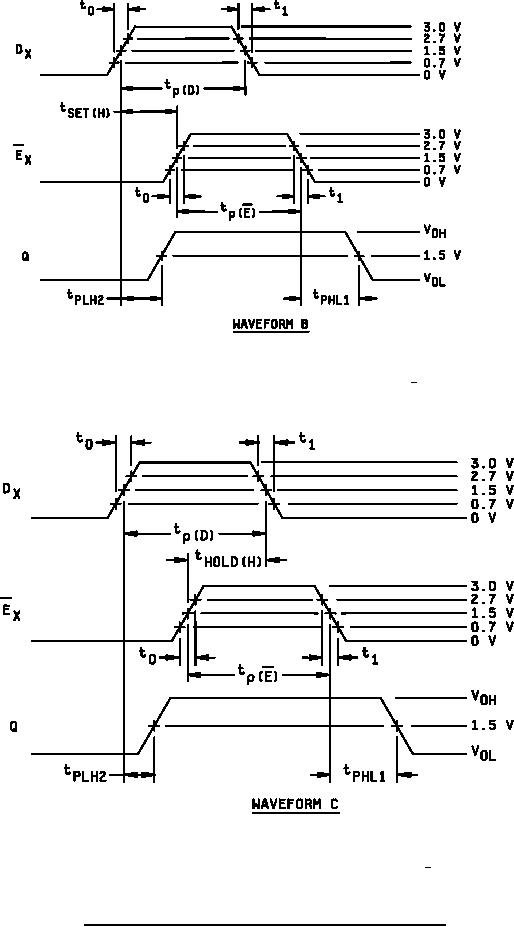
Figure 7. Switching time test circuit and waveforms for device type 04 waveform C |
|
||
| ||||||||||
|
|  MIL-M-38510/15B
NOTES:
1. The data inputs have the following characteristics: VGEN = 3 V, t0 = t1 ≤ 10 ns, tP(D) = 20 ns and PRR = 1 MHz.
2. The enable input has the following characteristics: VGEN = 3 V, t1 = t0 ≤ 10 ns, tP( E ) = 20 ns, tSET(H) = 5 ns,
PRR = 1 MHz and ZOUT ≈ 50Ω .
NOTES:
1. The data inputs have the following characteristics: VGEN = 3 V, t0 = t1 ≤ 10 ns, tP(D) = 20 ns and PRR = 1 MHz.
2. The enable inputs have the following characteristics: VGEN = 3 V, t1 = t0 ≤ 10 ns, tP( E ) = 20 ns, tHOLD(H) = 0 ns,
PRR = 1 MHz and ZOUT ≈ 50Ω .
Figure 7. Switching time test circuit and waveforms for device type 04.
18
|
|
Privacy Statement - Press Release - Copyright Information. - Contact Us |
