 |
|||
|
Page Title:
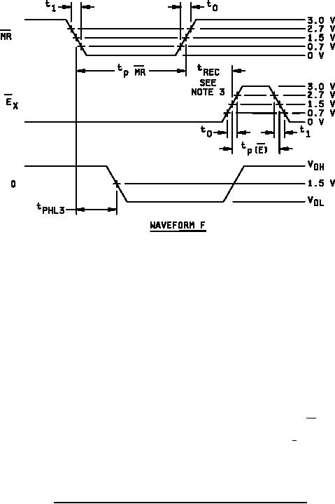
Figure 7. Switching time test circuit and waveforms for device type 04 waveform F |
|
||
| ||||||||||
|
|  MIL-M-38510/15B
NOTES:
1. The master reset input has the following characteristics: VGEN = 3 V, t0 = t1 ≤ 10 ns, tP( MR ) = 18 ns and PRR =
1 MHz.
2. The enable inputs have the following characteristics: VGEN = 3 V, t1 = t0 ≤ 10 ns, tP( E ) = 20 ns, tREC = 0 ns,
PRR = 1 MHz and ZOUT ≈ 50Ω .
3. Recovery time is the minimum time that enable must remain low after the master reset transition from low to
high in order for the latch to recognize and store high data.
Figure 7. Switching time test circuit and waveforms for device type 04.
20
|
|
Privacy Statement - Press Release - Copyright Information. - Contact Us |
