 |
|||
|
Page Title:
Table 1. Electrical performance characteristics. |
|
||
| ||||||||||
|
| 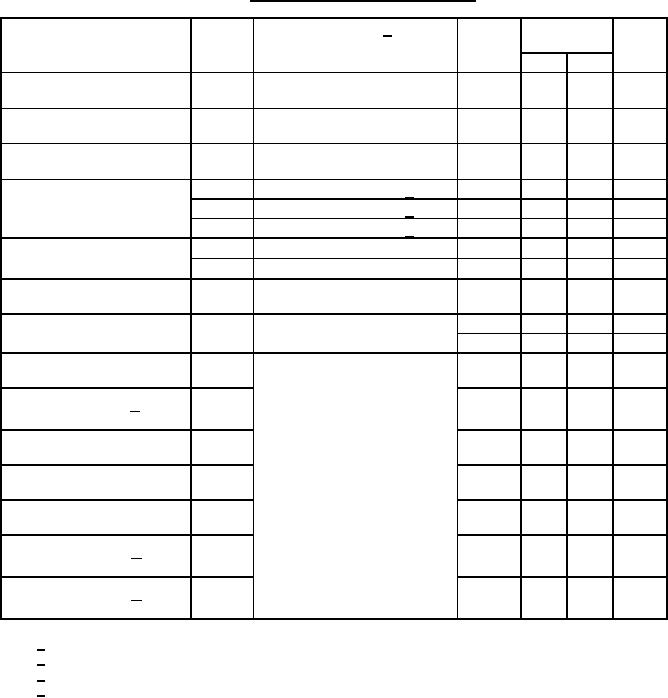 MIL-M-38510/17B
TABLE I. Electrical performance characteristics.
Conditions 1/
-55C ≤ TC ≤ +125C
Device
Limits
Unit
Test
Symbol
type
unless otherwise specified
Min
Max
All
2.4
V
High-level output voltage
VOH
VCC = 4.5 V;
IOH = -800 A
Low-level output voltage
VOL
VCC = 4.5 V; IIN = 16 mA
All
0.4
V
Input clamp voltage
VIC
VCC = 4.5 V; IIN = -12 mA;
All
-1.5
V
TC = 25C
Low-level input current
IIL1
VCC = 5.5 V; VIN = 0.4 V 2/
All
-0.3
-1.6
mA
IIL2
VCC = 5.5 V; VIN = 0.4 V 3/
All
-0.4
-1.6
mA
VCC = 5.5 V; VIN = 0.4 V 4/
All
-0.3
-0.8
mA
IIL3
A
High-level input current
IIH1
VCC = 5.5 V; VIN = 2.4 V
All
40
A
IIH2
VCC = 5.5 V; VIN = 5.5 V
All
100
Short-circuit output current
IOS
VCC = 5.5 V; VIN = 0
All
-20
-57
mA
Supply current per device
ICC
VCC = 5.5 V; VIN = 5.5 V
01
65
mA
02
45
mA
Maximum clock frequency
fMAX
VCC = 5 V;
All
25
MHz
CL = 50 pF 10%
RL = 390 Ω 5%
Propagation delay to high
02
5
36
ns
tPLH1
logic level (clear to Q )
Propagation delay to low
tPHL1
All
5
50
ns
logic level (clear to Q)
Propagation delay to high
tPLH2
All
5
43
ns
logic level (clock to Q)
Propagation delay to low
tPHL2
All
5
43
ns
logic level (clock to Q)
Propagation delay to high
02
5
43
ns
tPLH3
logic level (clock to Q )
tPHL3
Propagation delay to low
02
5
43
ns
logic level (clock to Q )
1/
See table III for complete terminal conditions.
2/
Clock input for device types 01 and 02.
3/
Clear input for device types 01 and 02.
4/
All D inputs for device types 01 and 02.
4
|
|
Privacy Statement - Press Release - Copyright Information. - Contact Us |
