 |
|||
|
Page Title:
Table 4B. Programming characteristics for circuit B |
|
||
| ||||||||||
|
| 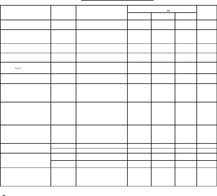 MIL-M-38510/203E
TABLE IVB. Programming characteristics for circuit B.
Limits 1/
Unit
Parameter
Symbol
Conditions
Min
Rec
Max
VCC required during
VCCP
5.4
5.5
5.6
V
programming
V/μs
Rise time of program
tTLH
0.34
0.40
0.46
pulse to data out or
program pin
Programming voltage on
VPP
32.5
33
33.5
V
program pin
Output programming
VOUT
25.5
26
26.5
V
voltage
μs
Programming pin pulse
Chip disabled, VCC = 5.5 V
----
100
180
tPP
width ( CE )
μs
Pulse width of
tP
Chip disabled, VCC = 5.5 V
1
----
40
programming voltage
240
----
----
mA
Required current limit of
IL
VPP = 33 V, VOUT = 26 V,
VCC = 5.5 V
power supply feeding
program pin and output
during programming
μs
Required time delay
TD1
Measured at 10% levels
70
80
90
between disabling
memory output and
application of output
programming pulse
Required time delay
TD2
Measured at 10% levels
100
ns
between removal of
programming pulse and
enabling memory output
Output current during
IOLV1
Chip enabled, VCC = 4.0 V
11
12
13
mA
verification
Chip enabled, VCC = 7.0 V
0.19
0.2
0.21
mA
IOLV2
Address input voltage
VIH
2.4
5.0
5.5
V
0.0
0.4
0.8
V
VIL
Maximum duty cycle
D. C.
tP/ tC
25
%
during automatic
programming of program
pin and output pin
1/ TC = +25C.
28
|
|
Privacy Statement - Press Release - Copyright Information. - Contact Us |
