 |
|||
|
Page Title:
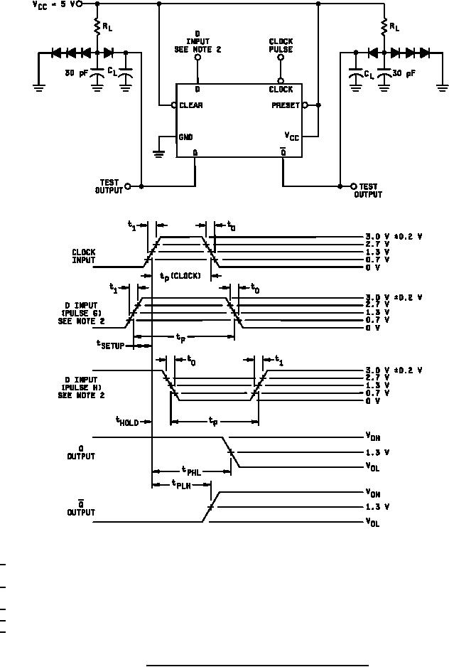
Figure 11. Synchronous switching test circuit for device type 05. |
|
||
| ||||||||||
|
|  MIL-M-38510/21F
NOTES:
1/ Clock input pulse has the following characteristics: Vgen = 3.0 V 0.2 V, t0 = 15 ns, t1 = 15 ns, tP = 200 ns,
PRR = 0.5 MHz, when testing fMAX, PRR = see table III.
2/ D input (pulse G and pulse H) has the following characteristics: Vgen = 3.0 V 0.2 V, t0 = 15 ns, t1 = 15 ns,
tSETUP = 50 ns, , tP = 100 ns and PRR is 50% of the clock PRR.
3/ All diodes are 1N916 or equivalent.
4/ CL = 50 pF minimum and includes probe and jig capacitance.
5/ RL = 4 kΩ 5%.
FIGURE 11. Synchronous switching test circuit for device type 05.
23
|
|
Privacy Statement - Press Release - Copyright Information. - Contact Us |
