 |
|||
|
Page Title:
Table 3. Group A inspection for device type 02-cont. |
|
||
| ||||||||||
|
| 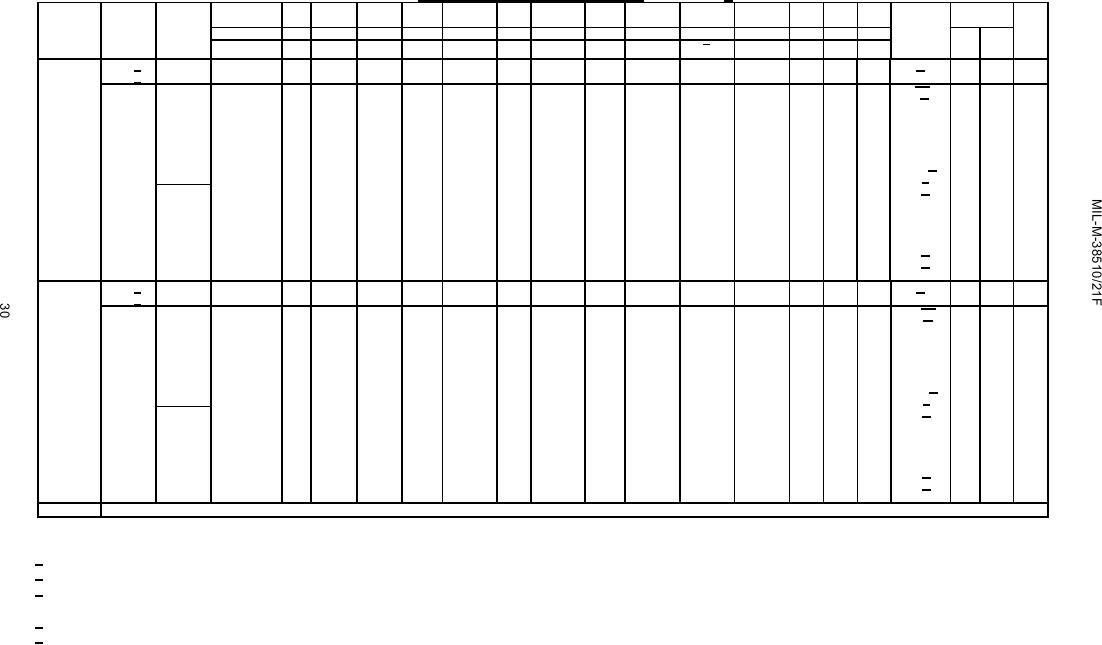 TABLE III. Group A inspection for device type 02 - Continued. 1/
Cases
1
2
3
4
5
6
7
8
9
10
11
12
13
14
Subgroup
Symbol
MIL-
A,B,D
Test limits
Measured
Unit
STD-883
terminal
Case C
9
12
13
14
2
1
3
4
5
6
7
8
10
11
Min Max
method
Test no.
K1
Clock
Preset
VCC
Clear
NC
J1
J2
J3
GND
Q
K2
K3
Q
(Fig. 5)
82
2.4 V
IN
B
5.0 V
5.0 V
2.4 V
2.4 V
2.4 V
GND
OUT 2.4 V 2.4 V
Q
9
fMAX 5/
3
MHz
TC =+25C
fMAX 5/
83
"
IN
B
"
5.0 V
"
"
"
OUT
"
"
"
Q
3
MHz
"
OUT
"
"
"
IN
"
J
2.4 V
Clear/Q
ns
"
"
75
*84 CKT A
"
10
3003
tPLH
"
OUT
"
"
"
IN
"
J
"
"
"
"
50
*84 CKT B
"
"
"
(Fig. 4)
Clear/Q
OUT
"
"
"
"
J
"
IN
"
"
"
"
75
*85 CKT A
"
"
"
Preset/Q
"
"
"
"
J
"
IN
"
"
"
"
50
*85 CKT B
"
"
"
Preset/Q
"
"
"
"
"
IN
"
J
GND
"
"
"
200
86 CKT A
"
"
tPHL
Clear/Q
"
"
"
"
"
IN
"
J
"
"
"
"
90
86 CKT B
"
"
Clear/Q_
"
"
"
OUT
"
"
"
J
"
IN
"
"
"
"
200
87 CKT A
"
"
Preset/Q
"
"
"
"
"
"
J
"
IN
"
"
"
"
90
87 CKT B
"
"
Preset/Q
"
"
"
"
"
"
5.0 V
"
J
IN
"
"
"
75
88 CKT A
"
"
Clock/Q
tPLH
3003
"
"
"
"
"
5.0 V
"
J
"
"
"
"
50
88 CKT B
"
"
"
Clock/Q
(Fig. 5)
"
"
"
"
J
"
5.0 V
"
"
"
"
75
89 CKT A
"
"
"
Clock/Q
OUT
"
"
"
"
J
"
5.0 V
"
"
"
"
50
89 CKT B
"
"
"
Clock/Q
"
"
"
"
"
5.0 V
"
J
"
"
"
"
150
90 CKT A
"
"
tPHL
Clock/Q
"
"
"
"
"
5.0 V
"
J
"
"
"
"
70
90 CKT B
"
"
Clock/Q
"
"
"
OUT
"
"
"
J
"
5.0 V
"
"
"
"
150
91 CKT A
"
"
Clock/Q
"
"
OUT
"
"
"
J
"
5.0 V
"
"
"
"
70
91 CKT B
"
"
Clock/Q
"
(Fig. 5)
92
"
"
B
"
5.0 V
"
"
"
"
OUT
"
"
Q
10
fMAX 5/
2.5
MHz
TC =+125C
fMAX 5/
93
"
"
B
"
5.0 V
"
"
"
OUT
"
"
"
Q
2.5
MHz
"
"
OUT
"
"
"
IN
"
J
2.4 V
ns
"
Clear/Q
125
*94 CKT A
"
tPLH
10
3003
"
"
OUT
"
"
"
IN
"
J
"
"
"
65
(Fig. 4) *94 CKT B
"
"
"
Clear/Q
"
OUT
"
"
"
"
J
"
IN
"
"
"
125
*95 CKT A
"
"
"
Preset/Q
"
"
"
"
"
"
J
"
IN
"
"
"
65
*95 CKT B
"
"
"
Preset/Q
"
"
"
"
"
"
IN
"
J
GND
"
"
250
96 CKT A
"
"
tPHL
Clear/Q
"
"
"
"
"
"
IN
"
J
"
"
"
100
96 CKT B
"
"
"
Clear/Q_
"
"
OUT
"
"
"
J
"
IN
"
"
"
250
97 CKT A
"
"
"
Preset/Q
"
"
"
"
"
"
J
"
IN
"
"
"
100
97 CKT B
"
"
Preset/Q
"
"
"
"
"
"
"
5.0 V
"
J
IN
"
"
125
98 CKT A
"
"
tPLH
Clock/Q
3003
"
"
"
"
"
5.0 V
"
J
"
"
"
65
(Fig. 5) 98 CKT B
"
"
"
"
Clock/Q
OUT
"
"
"
"
J
"
5.0 V
"
"
"
125
99 CKT A
"
"
"
"
Clock/Q
"
"
"
"
"
J
"
5.0 V
"
"
"
65
99 CKT B
"
"
"
"
Clock/Q
"
"
"
"
"
5.0 V
"
J
"
"
"
200
100 CKT A
"
"
"
tPHL
Clock/Q
"
"
"
"
"
5.0 V
"
J
"
"
"
85
100 CKT B
"
"
"
"
Clock/Q
"
OUT
"
"
"
J
"
5.0 V
"
"
"
200
101 CKT A
"
"
"
"
Clock/Q
"
OUT
"
"
"
J
"
5.0 V
"
"
"
85
101 CKT B
"
"
"
"
Clock/Q
Same tests, terminal conditions, and limits as for subgroup 10, except TC=-55C
11
NOTE: A = normal clock pulse, B = momentary GND, then 4.5 V.
J = input pulse, tp ≥ 100 ns, PRR = 0.5 MHz, VOL = 0 V, VOH = 4.5 V.
1/ Terminal conditions (pins not designated may be H ≥ 2.0 V, or L ≤ 0.8 V, or open).
2/ Tests shall be performed in sequence.
3/ Output voltages shall be either: (a) H = 2.4 V, minimum and L = 0.4 V, maximum when using a high speed checker double comparator; or
(b) H ≥ 1.5 V and L ≤ 1.5 V when using a high speed checker single comparator.
4/ Input voltages shown are: A = 2.4 V minimum and B = 0.4 V maximum.
5/ fMAX, minimum limit specified is the frequency of the input pulse. The output frequency shall be one-half of the input frequency.
*
These tests are performed at device manufacturer's option.
|
|
Privacy Statement - Press Release - Copyright Information. - Contact Us |
