 |
|||
|
Page Title:
Figure 5. Switching test circuit and waveforms for device type 05 |
|
||
| ||||||||||
|
| 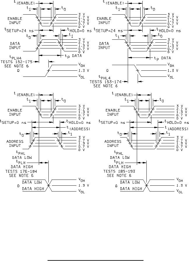 MIL-M-38510/316E
NOTES:
1. RL = 2 kΩ 5 percent.
2. CL = 50 pF 10% and includes probe and jig capacitance.
3. All loads are the same as the Q0 load.
4. All diodes are 1N3064 or equivalent.
5. The clear, enable, data, and address pulse generator have the following characteristics: VGEN = 3 V, t0 ≤ 15 ns,
t1 ≤ 6 ns, tP = 30 ns, and PRR ≤ 1 MHz except when measuring test nos. 152 thru 193, tP(ENABLE) = 24 ns,
tP(DATA) = 24 ns, tP(ADDRESS) = 24 ns, and tSETUP and tHOLD are as specified on the waveforms above.
6. Immediately prior to test 152, all outputs shall be cleared low; then beginning with test 152, test 152 thru 193 are
to be performed in sequence with a wait of 500 ns minimum between each test. These tests are to assure latchup
of the outputs under worst case setup and hold input conditions.
FIGURE 5. Switching test circuit and waveforms for device type 05 - Continued.
16
|
|
Privacy Statement - Press Release - Copyright Information. - Contact Us |
