 |
|||
|
Page Title:
Table 1. Electrical performance characteristics-cont. |
|
||
| ||||||||||
|
| 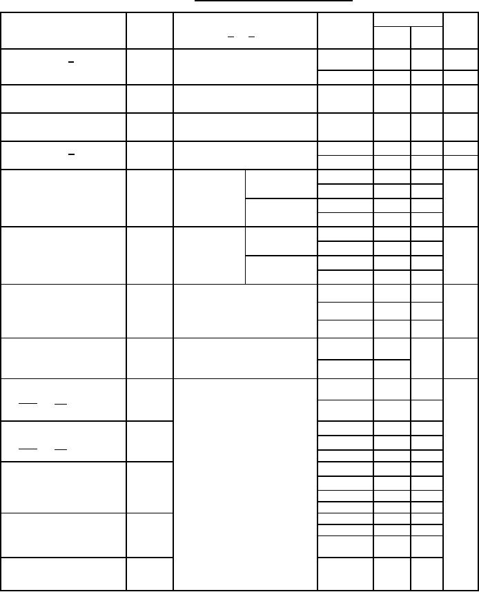 MIL-M-38510/371B
TABLE I. Electrical performance characteristics.
Limits
Test
Symbol
Conditions
Device
Unit
-55C < TC < +125C
types
Min
Max
unless otherwise specified
01, 02, 03,
mA
Output current 1/
IO
VCC = 5.5 V
-20
-112
04
VO = 2.25 V
05, 06, 07
mA
-15
-110
A
04, 05, 06,
Output current, high
IOZH
VCC = 5.5 V
20
07
level, outputs OFF
VO = 2.7 V
A
04, 05, 06,
Output current, low
IOZL
VCC = 5.5 V
-20
07
level, outputs OFF
VO = 0.4 V
01, 02
mA
4.0
Supply current 2/
ICC
VCC = 5.5 V
03
mA
VIN = 0 V
4.5
mA
05
17
Supply current, outputs
ICCH
VCC = 5.5 V
VIN = 5.0 V
high
04
18
06
15
VIN = 0 V
07
21
mA
04
27
Supply current, outputs
ICCL
VCC = 5.5 V
VIN = 0 V
low
06
29
05
23
VIN = 5.0 V
07
29
mA
05
27
Supply current, outputs
ICCZ
VCC = 5.5 V
VCC = 5.0 V
disabled
04
28
06, 07
31
01, 02, 04,
30
MHz
Maximum clock frequency
fmax
VCC = 5.0 V
05, 06, 07
CL = 50 pF 10%
03
25
RL = 500Ω
ns
Propagation delay time
VCC = 5.0 V
01, 02
3
15
tPLH1
CL = 50 pF 10%
low to high level,
RL = 500Ω
03
3
20
CLR or PR to output
Propagation delay time
01, 02
5
17
tPHL1
high to low,
03
4
22
CLR or PR to output
05, 07
6
22
Propagation delay time
01, 02
tPLH2
5
18
low to high level,
03
3
18
CLK to output
05, 06, 07
4
15
04
4
18
Propagation delay time
01, 02
5
20
tPHL2
high to low level,
03
5
23
CLK to output
04, 05,
4
15
06, 07
Propagation delay time
04, 05,
4
21
tPZL
output control to low
06, 07
level output
See footnotes at end of table.
6
|
|
Privacy Statement - Press Release - Copyright Information. - Contact Us |
