 |
|||
|
Page Title:
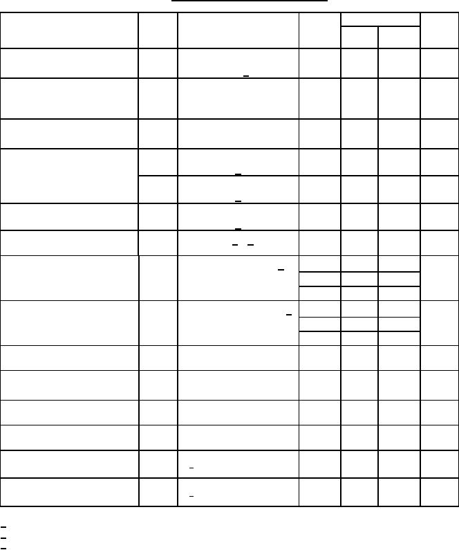
Table 1. Electrical performance characteristics. |
|
||
| ||||||||||
|
|  MIL-M-38510/40B
TABLE I. Electrical performance characteristics.
Test
Symbol
Conditions
Device
Unit
Limits
-55C ≤ TC ≤ +125C
type
Min
Max
unless otherwise specified
2.4
V
High level output voltage
All
VCC = 4.5 V, VIN = 0.8 V,
VOH
IOH = -500 A 1/
Low level output voltage
All
0.4
V
VCC = 4.5 V, IOL = 20 mA,
VOL
VIN = 2.0 V for all inputs of
gate under test
Input clamp voltage
All
-1.5
V
VCC = 4.5 V, IIN = -12 mA,
VIC
TC = +25C
A
All
50
High level input current
IIH1
VCC = 5.5 V, VIN = 2.4 V
2/
A
All
100
IIH2
VCC = 5.5 V, VIN = 5.5 V
2/
Low level input current
All
-1.0
-2.0
mA
VCC = 5.5 V, VIN = 0.4 V
IIL
1/
All
-40
-100
mA
Short circuit output current
VCC = 5.5 V 2/, 3/
IOS
01, 02
13
mA
High level supply current
VCC = 5.5 V, VIN = 0 V 2/
ICCH
03, 04
11
05
6.4
01, 02
24
mA
Low level supply current
VCC = 5.5 V, VIN = 5.5 V 1/
ICCL
03, 04
14
05
12
01, 03,
-5.85
mA
Expander input current
VCC = 4.5 V, VIN = 1.4 V
IX
05
Base emitter voltage of output
01, 03,
1.1
V
VCC = 4.5 V, IOL = 20 mA,
VBE
transistor
05
IX = 700 A
All
2
18
ns
Propagation delay time, high to
CL = 50 pF, RL = 280 Ω
tPHL1
low level expander pins open
All
2
18
ns
Propagation delay time, low to tPLH1
CL = 50 pF, RL = 280 Ω
high level expander pins open
Propagation delay time, high to
01, 03,
2
22
ns
CL = 50 pF, RL = 280 Ω
tPHL2
low level
05
C X = 15 pF
01, 03,
2
26
ns
Propagation delay time, low to
CL = 50 pF, RL = 280 Ω
tPLH2
05
high level
C X = 15 pF
1/ All unspecified inputs at 5.5 volts.
2/ All unspecified inputs grounded.
3/ Not more than one output should be shorted at a time.
4
|
|
Privacy Statement - Press Release - Copyright Information. - Contact Us |