 |
|||
|
Page Title:
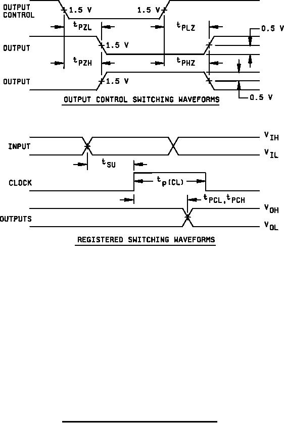
Figure 4. Switching time test circuit and waveforms-cont. |
|
||
| ||||||||||
|
|  MIL-M-38510/505C
NOTES:
1.
Test table for devices programmed in accordance with an altered item drawing may be
replaced by the equivalent tests which apply to the specific program configuration for the
resulting device.
CL = 45 pF minimum, including jig and probe capacitance; R1 = 390 Ω 5%; R2 = 750 Ω
2.
5%.
3.
Outputs may be under load simultaneously.
Requirements for tp (CL), tSU, and tH are established by setting parameters to the limits in table
4.
I and observing proper output state changes.
VIH = 3.0 V; VIL = 0.0 V.
5.
6.
For circuit C, the diode / VBIAS = 2.5 V may be replaced with switch S1, and VBIAS of 5.0 V.
S1 is open for tPZH, tPHZ, and Fmax tests.
FIGURE 4. Switching time test circuit and waveforms - Continued.
20
|
|
Privacy Statement - Press Release - Copyright Information. - Contact Us |
