 |
|||
|
Page Title:
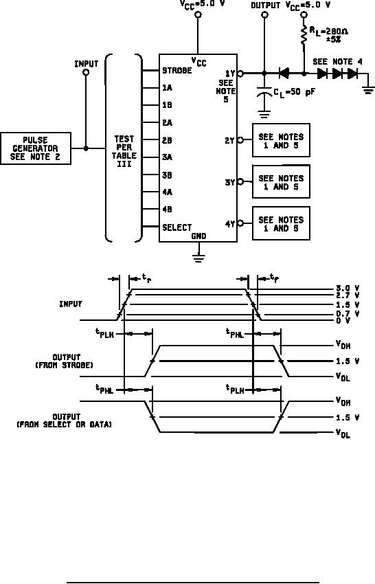
Figure 6. Switching time test circuits and waveforms for device type 04. |
|
||
| ||||||||||
|
|  MIL-M-38510/79D
NOTES:
1. Connect same load as shown for output 1Y.
≤
≤
≈
1 MHz, tr = tf
2.5 ns, and ZOUT
50 Ω.
2. The input pulse has the following characteristics: PRR
3.
CL includes probe and jig capacitance.
4.
All diodes are 1N3064 or equivalent.
5.
Load circuit is required on a given output only where table III indicates "OUT" on that output.
Load circuits may otherwise be omitted.
FIGURE 6. Switching time test circuits and waveforms for device type 04.
20
|
|
Privacy Statement - Press Release - Copyright Information. - Contact Us |
