 |
|||
|
Page Title:
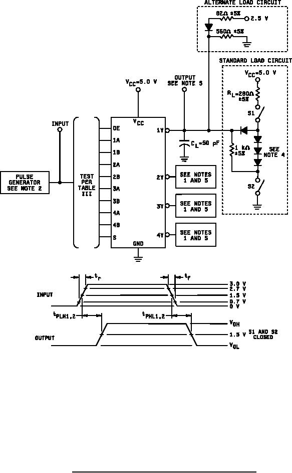
Figure 8. Switching time test circuits and waveforms for device type 06. |
|
||
| ||||||||||
|
|  MIL-M-38510/79D
NOTES:
1. Connect same load as shown for 1Y output.
≤
≤
≈
2. The input pulse has the following characteristics: tr = tf
2.5 ns, PRR
1 MHz, and ZOUT
50 Ω.
3.
CL includes probe and jig capacitance.
4.
All diodes are 1N3064 or equivalent.
5.
Load circuit is required on a given output only where table III indicates "OUT" on that output.
Load circuits may otherwise be omitted.
A.
Output 1 is for an output with internal conditions such that the output is low except when disabled
by the output control.
B. Output 2 is for an output with internal conditions such that the output is high except when disabled
by the output control.
6.
Manufacturer may test with either the standard load circuit or the alternate load circuit at his option.
FIGURE 8. Switching time test circuits and waveforms for device type 06.
23
|
|
Privacy Statement - Press Release - Copyright Information. - Contact Us |
