 |
|||
|
Page Title:
Figure 16. Transient response test circuit and waveform. |
|
||
| ||||||||||
|
| 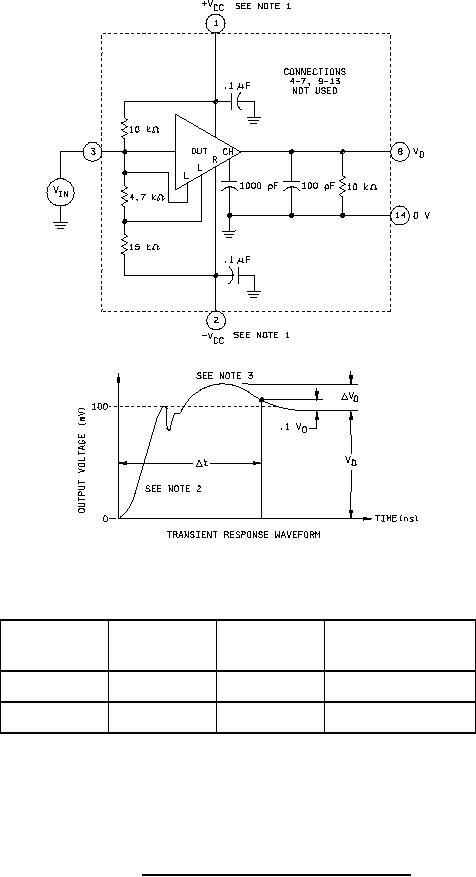 MIL-M-38510/125B
Input pulse
Output pulse
Parameter
signal at
signal
Equation
symbol
(see notes)
tr ≤ 50 ns
Above
100 mV
TR(ts) = Ćt
TR(ts)
waveform
Above
100 mV
TR(os) = ĆVO / VO
TR(os)
waveform
NOTES:
1. +VCC and VCC shall be at the common mode limits.
(For example: first +3.5 V, -26.5 V and then +26.5 V, -3.5 V.)
2. Any high frequency ringing shall be over within 2 s.
3. After its peak the major loop response shall be without further oscillations.
FIGURE 16. Transient response test circuit and waveform.
26
|
|
Privacy Statement - Press Release - Copyright Information. - Contact Us |
