 |
|||
|
Page Title:
Table III. Group A inspection for device type 02-cont. |
|
||
| ||||||||||
|
|  1/
Cases 2 and X pins not referenced are N/C.
2/
Apply all voltages, then apply 3 V, 0 V, 3 V to SD X, then apply 3 V, 0 V, 3 V to CPX, then make measurement. For circuit C devices, apply all voltages
then apply 4.5 V, 0 V, 4.5 V to SD X. then apply 4.5 V, 0 V, 4.5 V to CPX, then make the measurement.
3/
Apply all voltages, then apply 3 V, 0 V, 3 V to CD X, then apply 3 V, 0 V, 3 V to CPX, then make measurement. For circuit C devices, apply all voltages
then apply 4.5 V, 0 V, 4.5 V to CP X, then make the measurement.
4/
Apply all voltages, then apply 0 V, 4.5 V to CPX, CDX, or SDX, then make measurement.
5/
Apply all voltages, then apply 0 V, 4.5 V, 0 V to CP1 test 32 and 44 and CP2 test 33 and 45 then make measurement.
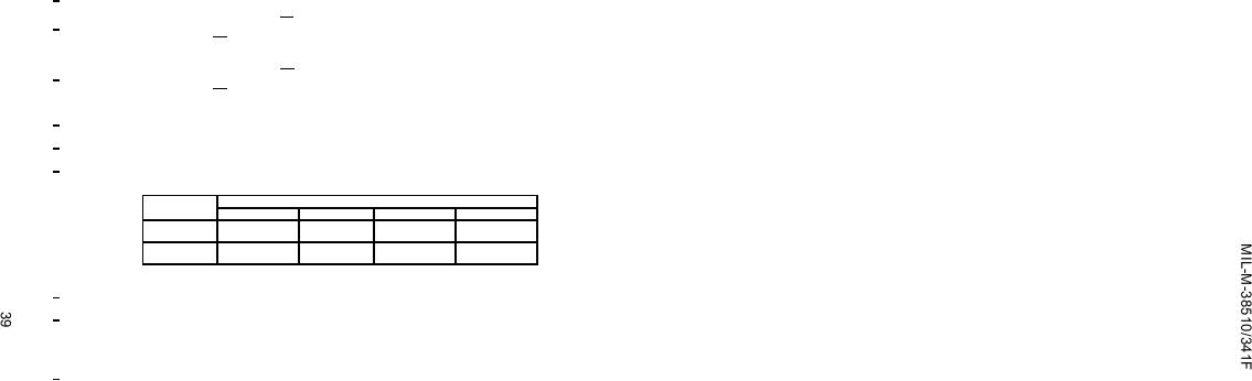
6/
IIL limits (mA) min/max values for circuits shown:
Circuits
Parameter
A
B
C
D
IIL1
-.25/-.60
-.03/-.60
-.03/-.60
-.03/-.60
IIL2
-.75/-1.80
-.09/-1.80
-.09/-1.80
-.09/-1.80
7/
Perform function sequence at VCC = 4.5 V and repeat at VCC = 5.5 V.
8/
A = 2.5 V
B = 0.5 V
H ≥ 1.5 V
L ≤ 1.5 V
9/
fMAX minimum limit specified is the frequency of the input pulse. The output frequency shall be one-half of the input frequency.
|
|
Privacy Statement - Press Release - Copyright Information. - Contact Us |
