 |
|||
|
Page Title:
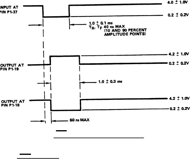
Figure 2. Video input and output signal waveforms. |
|
||
| ||||||||||
|
|  MIL-C-62204B(AR)
FIGURE 2. Video input and output signal waveforms.
3.3.4 HALF
signal.
a. With the logical one digital type-A signal (item 3.1 of table I)
present between pins P1-35 ad P1-7 ad pins P1-37 and P1-7, and
with a logical zero digital type-A signal (item 3.1 of table I)
applied momentarily between pins P1-14 and P1-7, the output
voltages between pins P1-32 and P1-7 and pins P2-9 and P1-7 shall
be 0.2 0.2V. With subsequent momentary application of a logical
zero digital type-A signal between pins P1-33 and P1-7, the
voltages between pins P1-32 and P1-7 and pins P2-9 and P1-7 shall
change to 4.2 1.0V.
8
|
|
Privacy Statement - Press Release - Copyright Information. - Contact Us |
