 |
|||
|
Page Title:
Figure 3. MALF 3 input signal waveforms. |
|
||
| ||||||||||
|
| 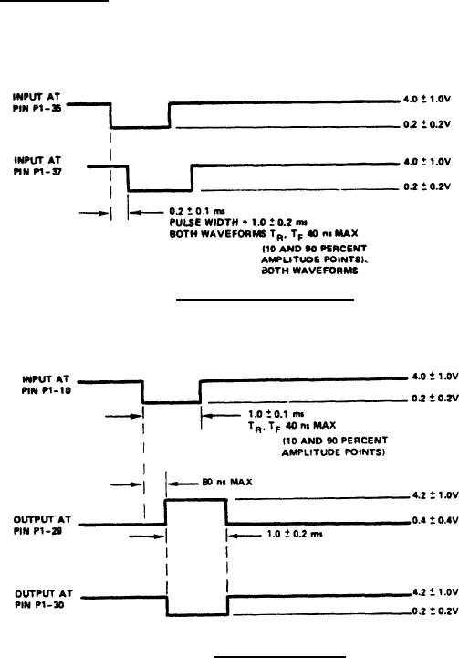 MIL-C-62205B(AR)
b. With the output voltages between pins P1-32 and P1-7 and pins P2-9
and P1-7 established at 0.2 0.2V as specified in 3.3.l.4a, with
application of digital type-A signals between pins P2-35 and P1-7
and pins P1-37 and P1-7 as specified on figure 3, the voltages
between pins P1-32 and P1-7 and pins P2-9 and P1-7 shall change
to 4.2 1.0V. (See 4.6.2.4)
3.3.5 Reset signal. With the digital type-A signal (item 3.1 of Table I)
applied between pins P1-10 and P1-7 as specified on figure 4, the outputs
between pins P1-29 and P1-7 and pins P1-30 and P1-7 shall be as specified on
figure 4. (See 4.6.2.5)
FIGURE 3. MALF 3 input signal waveforms.
FIGURE 4, Reset signal waveforms.
9
|
|
Privacy Statement - Press Release - Copyright Information. - Contact Us |
